RD3172MMA7455L Freescale Semiconductor, RD3172MMA7455L Datasheet - Page 15
RD3172MMA7455L
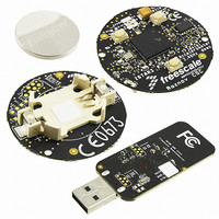
Manufacturer Part Number
RD3172MMA7455L
Description
EVAL BOARD FOR MMA7455L
Manufacturer
Freescale Semiconductor
Series
ZSTAR3r
Datasheets
1.RD3172MMA7455L.pdf
(35 pages)
2.RD3172MMA7455L.pdf
(2 pages)
3.RD3172MMA7455L.pdf
(100 pages)
Specifications of RD3172MMA7455L
Design Resources
ZSTAR3 Schematic
Sensor Type
Accelerometer, 3 Axis
Sensing Range
±2g, 4g, 8g
Interface
RF
Sensitivity
16, 32, 64 LSB/g
Voltage - Supply
3V
Embedded
Yes, MCU, 16-Bit
Utilized Ic / Part
MMA7455
Acceleration
5000 g
Sensing Axis
Triple Axis
Output Type
Digital
Interface Type
I2C, SPI
Operating Voltage
3.6 L
Operating Current
490 uA
Maximum Operating Temperature
+ 85 C
Minimum Operating Temperature
- 40 C
Lead Free Status / RoHS Status
Lead free / RoHS Compliant
For Use With/related Products
MMA7455L
Available stocks
Company
Part Number
Manufacturer
Quantity
Price
Company:

Part Number:
RD3172MMA7455L
Manufacturer:
Freescale Semiconductor
Quantity:
135


ASSIGNING, CLEARING & DETECTING INTERRUPTS
Assigning the interrupt pins is done in Register $18. There are 3 combinations for the interrupt pins to be assigned which are
outlined below in the table for INTREG[1:0].
Table 7. Configuring the Interrupt settings using Register $18 with INTREG[1:0] bits
00: INT1 Register is detecting Level while INT2 is detecting Pulse.
01: INT1 Register is detecting Pulse while INT2 is detecting Level.
10: INT1 Register is detecting a Single Pulse and INT2 is detecting Single Pulse (if 2
time window and second time window > 0 then INT2 will detect the double pulse only.
INTPIN: INT1 pin is routed to INT1 bit in Detection Source Register ($0A) and INT2 pin is routed to INT2 bit in Detection Source
Register ($0A).
INTPIN: INT2 pin is routed to INT1 bit in Detection Source Register ($0A) and INT1 pin is routed to INT2 bit in Detection Source
Register ($0A).
Note: When INTREG[1:0] =10 for the condition to detect single pulse on INT1 and either single or double pulse on INT2, INT1
register bit can no longer be cleared by setting CLR_INT1 bit. It is cleared by setting CLR_INT2 bit. In this case, setting CLR_INT2
clears both INT1 and INT2 register bits and resets the detection operation. Follow the example given for clearing the interrupts.
Clearing the Interrupt Pins: Register $17
CLR_INT1
1: Clear “INT1”
0: Do not clear “INT1”
CLR_INT2
1: Clear “INT2”
0: Do not clear “INT2”
After interrupt has triggered due to a detection, the interrupt pin (INT1 or INT2) need to be cleared by writing a logic 1. Then the
interrupt pin should be enabled to trigger the next detection by setting it to a logic 0.
This example is to show how to reset the interrupt flags
void ClearIntLatch(void)
{
IIC_ByteWrite(INTRST, 0x03);
IIC_ByteWrite(INTRST, 0x00);
}
$18 Control 1 Register
$17: Interrupt Latch Reset (Read/Write)
Sensors
Freescale Semiconductor
DFBW
D7
D7
0
--
0
INTREG[1:0]
00
01
10
THOPT
D6
D6
--
0
0
ZDA
D5
D5
--
0
0
Single Pulse detection
“INT1” Register Bit
Pulse Detection
Level detection
YDA
D4
D4
--
0
0
XDA
D3
D3
--
0
0
INTREG[1]
D2
D2
--
0
0
nd
INTREG[0]
Time Window = 0) or if there is a latency
CLR_INT2
Single or Double Pulse Detection
D1
D1
0
0
“INT2” Register Bit
Pulse Detection
Level Detection
CLR_INT1
INTPIN
D0
D0
0
0
MMA7455L
Function
Function
Reg $18
Reg $17
Default
Default
15
Related parts for RD3172MMA7455L
Image
Part Number
Description
Manufacturer
Datasheet
Request
R

Part Number:
Description:
Manufacturer:
Freescale Semiconductor, Inc
Datasheet:
Part Number:
Description:
Manufacturer:
Freescale Semiconductor, Inc
Datasheet:
Part Number:
Description:
Manufacturer:
Freescale Semiconductor, Inc
Datasheet:
Part Number:
Description:
Manufacturer:
Freescale Semiconductor, Inc
Datasheet:
Part Number:
Description:
Manufacturer:
Freescale Semiconductor, Inc
Datasheet:
Part Number:
Description:
Manufacturer:
Freescale Semiconductor, Inc
Datasheet:
Part Number:
Description:
Manufacturer:
Freescale Semiconductor, Inc
Datasheet:
Part Number:
Description:
Manufacturer:
Freescale Semiconductor, Inc
Datasheet:
Part Number:
Description:
Manufacturer:
Freescale Semiconductor, Inc
Datasheet:
Part Number:
Description:
Manufacturer:
Freescale Semiconductor, Inc
Datasheet:
Part Number:
Description:
Manufacturer:
Freescale Semiconductor, Inc
Datasheet:
Part Number:
Description:
Manufacturer:
Freescale Semiconductor, Inc
Datasheet:
Part Number:
Description:
Manufacturer:
Freescale Semiconductor, Inc
Datasheet:
Part Number:
Description:
Manufacturer:
Freescale Semiconductor, Inc
Datasheet:
Part Number:
Description:
Manufacturer:
Freescale Semiconductor, Inc
Datasheet: