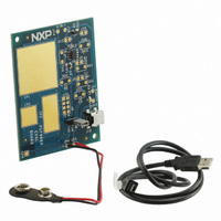
OM11055 NXP Semiconductors, OM11055 Datasheet - Page 19

OM11055
Manufacturer Part Number
OM11055
Description
EVAL BOARD FOR PCF8883
Manufacturer
NXP Semiconductors
Specifications of OM11055
Sensor Type
Capacitive
Interface
Mini USB
Voltage - Supply
3 V ~ 9 V
Embedded
No
Utilized Ic / Part
PCF8883
Lead Free Status / RoHS Status
Lead free / RoHS Compliant
Sensitivity
-
Sensing Range
-
Other names
568-4958
Available stocks
Company
Part Number
Manufacturer
Quantity
Price
Company:
Part Number:
OM11055
Manufacturer:
NXP Semiconductors
Quantity:
135
Company:
Part Number:
OM11055598
Manufacturer:
NXP Semiconductors
Quantity:
135
NXP Semiconductors
15. Soldering of SMD packages
PCF8883
Product data sheet
15.1 Introduction to soldering
15.2 Wave and reflow soldering
This text provides a very brief insight into a complex technology. A more in-depth account
of soldering ICs can be found in Application Note AN10365 “Surface mount reflow
soldering description”.
Soldering is one of the most common methods through which packages are attached to
Printed Circuit Boards (PCBs), to form electrical circuits. The soldered joint provides both
the mechanical and the electrical connection. There is no single soldering method that is
ideal for all IC packages. Wave soldering is often preferred when through-hole and
Surface Mount Devices (SMDs) are mixed on one printed wiring board; however, it is not
suitable for fine pitch SMDs. Reflow soldering is ideal for the small pitches and high
densities that come with increased miniaturization.
Wave soldering is a joining technology in which the joints are made by solder coming from
a standing wave of liquid solder. The wave soldering process is suitable for the following:
Not all SMDs can be wave soldered. Packages with solder balls, and some leadless
packages which have solder lands underneath the body, cannot be wave soldered. Also,
leaded SMDs with leads having a pitch smaller than ~0.6 mm cannot be wave soldered,
due to an increased probability of bridging.
The reflow soldering process involves applying solder paste to a board, followed by
component placement and exposure to a temperature profile. Leaded packages,
packages with solder balls, and leadless packages are all reflow solderable.
Key characteristics in both wave and reflow soldering are:
Fig 17. Three dimensional package drawing of PCF8883 (SOIC8)
•
•
•
•
•
•
•
•
Through-hole components
Leaded or leadless SMDs, which are glued to the surface of the printed circuit board
Board specifications, including the board finish, solder masks and vias
Package footprints, including solder thieves and orientation
The moisture sensitivity level of the packages
Package placement
Inspection and repair
Lead-free soldering versus SnPb soldering
All information provided in this document is subject to legal disclaimers.
Rev. 2 — 8 March 2011
Capacitive proximity switch with auto-calibration
PCF8883
© NXP B.V. 2011. All rights reserved.
19 of 25


