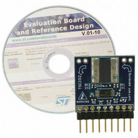
STEVAL-ISQ010V1 STMicroelectronics, STEVAL-ISQ010V1 Datasheet

STEVAL-ISQ010V1
Specifications of STEVAL-ISQ010V1
Available stocks
Related parts for STEVAL-ISQ010V1
STEVAL-ISQ010V1 Summary of contents
Page 1
High-side current sense amplifier plus signal conditioning amplifier Features ■ Independent supply and input common-mode voltages ■ Wide common-mode operating range: 2 ■ Wide common-mode surviving range: - (reversed battery and load-dump conditions) ■ ...
Page 2
Contents Contents 1 Application schematic and pin description . . . . . . . . . . . . . . . . . . . . . . 3 2 Absolute maximum ratings and operating conditions . . ...
Page 3
TSC102 1 Application schematic and pin description The TSC102 high-side current sense amplifier features a 2 input common-mode range that is independent of the supply voltage. The main advantage of this feature is that it allows high-side ...
Page 4
Absolute maximum ratings and operating conditions 2 Absolute maximum ratings and operating conditions Table 2. Absolute maximum ratings Symbol V Input pins differential voltage ( Current sensing input pin voltages ( Voltage for pins A1, A2, ...
Page 5
TSC102 3 Electrical characteristics Unless otherwise specified, the electrical characteristics given in the following tables have been measured under the following test conditions. ● 25° amb ● No load on Out pin. ● Signal conditioning amplifier ...
Page 6
Electrical characteristics Table 6. Current sensing amplifier output stage Symbol Parameter Gain Av (variation of V versus node high-level saturation V voltage oh1 oh1 node low-level saturation V ol1 voltage ...
Page 7
TSC102 Table 9. Signal conditioning amplifier Symbol Parameter V Common mode voltage range icm V Input offset voltage IO ΔV Input offset voltage drift IO Iib Input bias current Output high-level saturation V oh2 voltage ( oh2 ...
Page 8
Electrical characteristics curves: current sense amplifier 4 Electrical characteristics curves: current sense amplifier Unless otherwise specified, the test conditions for the following curves are: ● 25° amb ● no load on Out pin. ● signal conditioning ...
Page 9
TSC102 Figure 6. Vp pin input bias current vs. Vsense T=-40° -250 -150 -50 Vsense (mV) Figure 8. Output stage low-state saturation voltage versus output current (Vsense = -1 V) 1200 ...
Page 10
Electrical characteristics curves: current sense amplifier Figure 12. Bode diagram -10 -20 -30 10/24 Figure 13. Power supply rejection ratio 100 Doc ID 16754 Rev 2 ...
Page 11
TSC102 5 Electrical characteristics curves: signal conditioning amplifier Unless otherwise specified, the test conditions for the following curves are: ● 25° amb ● no load on Out. ● signal conditioning amplifier tested as standalone amplifier. Figure ...
Page 12
Parameter definitions 6 Parameter definitions 6.1 Common-mode rejection ratio (CMR) The common-mode rejection ratio (CMR) measures the ability of the current sensing amplifier to reject any DC voltage applied on both inputs V back to the input so that its ...
Page 13
TSC102 Figure 18. V versus V a1 6.4 Output voltage drift versus temperature The output voltage drift versus temperature is defined as the maximum variation of V respect to its value at 25° C, over the temperature range ...
Page 14
Parameter definitions Figure 19. Output voltage drift versus temperature 6.5 Output voltage accuracy The output voltage accuracy is the difference between the actual output voltage and the theoretical output voltage. Ideally, the current sensing output voltage should be equal to ...
Page 15
TSC102 Figure 20 The output voltage accuracy, expressed as a percentage, can be calculated with the following formula: with V/V. vs. V theoretical and actual characteristics sense Va1 Va1 abs ...
Page 16
Application information 7 Application information The TSC102 can be used to measure current and feed back the information to a microcontroller, as shown in Figure 21. Typical application schematic Iload Vp 8 Rsense Vm 1 Vsense Gnd 2 load This ...
Page 17
TSC102 Figure 23. Gain lower than 20 Vsense Figure 24. Overcurrent protection Vsense TSC102 Gnd Vcc TSC102 Gnd ...
Page 18
Application information Figure 25. First-order low-pass filter Vsense Figure 26. Second-order low-pass filter Vsense 18/24 TSC102 Gnd Vcc TSC102 Gnd ...
Page 19
TSC102 8 Package information In order to meet environmental requirements, ST offers these devices in different grades of ® ECOPACK packages, depending on their level of environmental compliance. ECOPACK specifications, grade definitions and product status are available at: www.st.com. ® ...
Page 20
Package information 8.1 SO-8 package information Figure 27. SO-8 package mechanical drawing Table 10. SO-8 package mechanical data Ref ccc 20/24 Dimensions Millimeters Min. Typ. Max. 1.75 ...
Page 21
TSC102 8.2 TSSOP-8 package information Figure 28. TSSOP8 package mechanical drawing Table 11. TSSOP8 package mechanical data Ref aaa Dimensions Millimeters Min. Typ. Max. 1.20 0.05 0.15 0.80 ...
Page 22
Ordering information 9 Ordering information Table 12. Order codes Part number TSC102IPT TSC102IDT TSC102IYPT TSC102IYDT 1. Qualification and characterization according to AEC Q100 and Q003 or equivalent, advanced screening according to AEC Q001 & Q 002 or equivalent are on-going. ...
Page 23
TSC102 10 Revision history Table 13. Document revision history Date 09-Nov-2009 03-Mar-2011 Revision 1 Initial release. Added automotive grade qualification for SO-8 package 2 (note 2. under Table Doc ID 16754 Rev 2 Revision history Changes 12). 23/24 ...
Page 24
... Information in this document is provided solely in connection with ST products. STMicroelectronics NV and its subsidiaries (“ST”) reserve the right to make changes, corrections, modifications or improvements, to this document, and the products and services described herein at any time, without notice. All ST products are sold pursuant to ST’s terms and conditions of sale. ...


