STEVAL-ISQ007V1 STMicroelectronics, STEVAL-ISQ007V1 Datasheet - Page 11
STEVAL-ISQ007V1
Manufacturer Part Number
STEVAL-ISQ007V1
Description
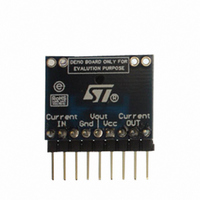
BOARD EVAL BASED ON TSC101
Manufacturer
STMicroelectronics
Type
Other Power Managementr
Specifications of STEVAL-ISQ007V1
Channels Per Ic
1 - Single
Amplifier Type
Current Sense
Output Type
Single-Ended
Slew Rate
0.9 V/µs
-3db Bandwidth
450kHz
Current - Output / Channel
60mA
Operating Temperature
-40°C ~ 125°C
Current - Supply (main Ic)
165µA
Voltage - Supply, Single/dual (±)
4 V ~ 24 V
Board Type
Fully Populated
Utilized Ic / Part
TSC101
Input Voltage
4 V to 24 V
Product
Power Management Modules
Silicon Manufacturer
ST Micro
Silicon Core Number
TSC101
Kit Application Type
Amplifier
Application Sub Type
Current-Sense Amplifier
Kit Contents
Board
Rohs Compliant
Yes
Lead Free Status / RoHS Status
Lead free / RoHS Compliant
For Use With/related Products
TSC101
Other names
497-8339
Available stocks
Company
Part Number
Manufacturer
Quantity
Price
Company:

Part Number:
STEVAL-ISQ007V1
Manufacturer:
STMicroelectronics
Quantity:
1


TSC101
4
4.1
4.2
4.3
Parameter definitions
Common mode rejection ratio (CMR)
The common-mode rejection ratio (CMR) measures the ability of the current-sensing
amplifier to reject any DC voltage applied on both inputs V
back to the input so that its effect can be compared with the applied differential signal. The
CMR is defined by the formula:
Supply voltage rejection ratio (SVR)
The supply-voltage rejection ratio (SVR) measures the ability of the current-sensing
amplifier to reject any variation of the supply voltage V
input so that its effect can be compared with the applied differential signal. The SVR is
defined by the formula:
Gain (Av) and input offset voltage (V
The input offset voltage is defined as the intersection between the linear regression of the
V
V
can be calculated with the following formula:
The amplification gain A
voltage:
out
sense
versus V
=V
sense1
sense
=50mV and V
curve with the X-axis (see
V
os
v
=
is defined as the ratio between output voltage and input differential
SVR
V
CMR
sense1
out2
Doc ID 13313 Rev 3
=
is the output voltage with V
=
–
–
Av
20
–
⎛
⎝
20
V
----------------------------------------------- -
⋅
=
sense1
V
⋅
log
----------------- -
V
out1
log
V
sense
----------------------------- -
ΔV
out
------------------------------
ΔV
–
–
ΔV
CC
Figure
V
V
ΔV
icm
sense2
out2
out
⋅
out
⋅
Av
Av
20). If V
⋅
CC
os
V
. The SVR is referred back to the
out1
)
p
and V
sense
out1
⎞
⎠
is the output voltage with
=V
m
. The CMR is referred
sense2
Parameter definitions
=5mV, then V
11/18
os
Related parts for STEVAL-ISQ007V1
Image
Part Number
Description
Manufacturer
Datasheet
Request
R

Part Number:
Description:
BOARD RGB CTR ST7,STP08C596MTR
Manufacturer:
STMicroelectronics
Datasheet:

Part Number:
Description:
Power Management IC Development Tools Full Speed USB to RS232 Bridge Demo
Manufacturer:
STMicroelectronics
Datasheet:
Part Number:
Description:
Power Management IC Development Tools 2.5W solar eval BRD USB SPV1040 LD39050
Manufacturer:
STMicroelectronics
Datasheet:

Part Number:
Description:
BOARD EVAL FOR MEMS SENSORS
Manufacturer:
STMicroelectronics
Datasheet:

Part Number:
Description:
KIT DEV STARTER ST10F276Z5
Manufacturer:
STMicroelectronics
Datasheet:

Part Number:
Description:
BOARD EVAL HDMI $ VIDEO SWITCH
Manufacturer:
STMicroelectronics
Datasheet:

Part Number:
Description:
BOARD DEMO ACCELEROMETER DIL24
Manufacturer:
STMicroelectronics
Datasheet:

Part Number:
Description:
BOARD STLM75/STDS75/ST72F651
Manufacturer:
STMicroelectronics
Datasheet:

Part Number:
Description:
EVAL BOARD 3AXIS MEMS ACCELLRMTR
Manufacturer:
STMicroelectronics
Datasheet:

Part Number:
Description:
BOARD EVAL 8BIT MICRO + TDE1708
Manufacturer:
STMicroelectronics
Datasheet:
Part Number:
Description:
STMicroelectronics [RIPPLE-CARRY BINARY COUNTER/DIVIDERS]
Manufacturer:
STMicroelectronics
Datasheet:
Part Number:
Description:
STMicroelectronics [LIQUID-CRYSTAL DISPLAY DRIVERS]
Manufacturer:
STMicroelectronics
Datasheet:
Part Number:
Description:
BOARD EVAL FOR MEMS SENSORS
Manufacturer:
STMicroelectronics
Datasheet: