MCP6S22DM-PICTL Microchip Technology, MCP6S22DM-PICTL Datasheet - Page 25
MCP6S22DM-PICTL
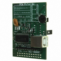
Manufacturer Part Number
MCP6S22DM-PICTL
Description
BOARD DEMO FOR MCP6S22
Manufacturer
Microchip Technology
Series
PICtail™r
Specifications of MCP6S22DM-PICTL
Channels Per Ic
2 - Dual
Amplifier Type
Programmable Gain
Output Type
Single-Ended, Rail-to-Rail
Slew Rate
22 V/µs
-3db Bandwidth
12MHz
Current - Output / Channel
30mA
Operating Temperature
-40°C ~ 85°C
Current - Supply (main Ic)
1mA
Voltage - Supply, Single/dual (±)
2.5 V ~ 5.5 V
Board Type
Fully Populated
Utilized Ic / Part
MCP6S22
Lead Free Status / RoHS Status
Contains lead / RoHS non-compliant
Available stocks
Company
Part Number
Manufacturer
Quantity
Price

Part Number:
MCP6S22DM-PICTL
Manufacturer:
MICROCHIP/微芯
Quantity:
20 000


6.0
6.1
Figure 6-1 shows a MCP6S21 with the V
2.5V and V
signals centered on 2.5V, instead of ground-referenced
signals. The voltage reference MCP1525 is buffered by
a MCP6021, which gives a low output impedance ref-
erence voltage from DC to high frequencies. The
source driving the V
impedance of
accuracy.
FIGURE 6-1:
Reference Voltage.
6.2
Large capacitive loads can cause both stability prob-
lems and reduced bandwidth for the MCP6S21/2/6/8
family of PGAs (Figure 2-17 and Figure 2-18). This
happens because a large load capacitance decreases
the internal amplifier’s phase margin and bandwidth.
Figure 6-2 can be used. A small series resistor (R
at the V
load resistive at high frequencies. It will not, however,
improve the bandwidth.
FIGURE 6-2:
Capacitive Loads.
If the PGA drives a large capacitive load, the circuit in
2003 Microchip Technology Inc.
V
IN
2.5V
REF
V
DD
OUT
APPLICATIONS INFORMATION
MCP1525
Changing External Reference
Voltage
Capacitive Load and Stability
1 µF
DD
improves the phase margin by making the
MCP6S2X
= 5.0V. This allows the PGA to amplify
MCP6021
0.1
REF
PGA with Different External
PGA Circuit for Large
V
V
to maintain reasonable gain
DD
IN
pin should have an output
R
MCP6S21
V
ISO
REF
V
DD
C
REF
L
V
V
OUT
OUT
pin at
ISO
)
For C
value can be fine-tuned on the bench. Adjust R
that the step response overshoot and frequency
response peaking are acceptable at all gains.
6.3
Good PC board layout techniques will help achieve the
performance shown in the Electrical Characteristics
and Typical Performance Curves. It will also help
minimize EMC (Electro-Magnetic Compatibility) issues.
6.3.1
Separate circuit functions; digital from analog, low
speed from high speed, and low power from high
power, as this will reduce crosstalk.
Keep sensitive traces short and straight, separating
them from interfering components and traces. This is
especially important for high frequency (low rise time)
signals.
Use a 0.1 µF supply bypass capacitor within 0.1 inch
(2.5 mm) of the V
ground plane. A multi-layer ceramic chip capacitor, or
high-frequency equivalent, works best.
6.3.2
The input pins of the MCP6S21/2/6/8 family of opera-
tional amplifiers (op amps) are high-impedance. This
makes them especially susceptible to capacitively-cou-
pled noise. Using a ground plane helps reduce this
problem.
When noise is capacitively-coupled, the ground plane
provides additional shunt capacitance to ground. When
noise is magnetically coupled, the ground plane
reduces the mutual inductance between traces.
Increasing the separation between traces makes a
significant difference.
Changing the direction of one of the traces can also
reduce magnetic coupling. It may help to locate guard
traces next to the victim trace. They should be on both
sides of the victim trace and be as close as possible.
Connect the guard traces to the ground plane at both
ends, and in the middle, of long traces.
6.3.3
Because the MCP6S21/2/6/8 PGAs reach unity gain
near 64 MHz when G = 16 and 32, it is important to use
good PCB layout techniques. Any parasitic coupling at
high frequency might cause undesired peaking. Filter-
ing high frequency signals (i.e., fast edge rates) can
help. To minimize high frequency problems:
• Use complete ground and power planes
• Use HF, surface mount components
• Provide clean supply voltages and bypassing
• Keep traces short and straight
• Try a linear power supply (e.g., an LDO)
L
100 pF, a good estimate for R
Layout Considerations
COMPONENT PLACEMENT
SIGNAL COUPLING
HIGH FREQUENCY ISSUES
MCP6S21/2/6/8
DD
pin. It must connect directly to the
DS21117A-page 25
ISO
is 50 . This
ISO
so
Related parts for MCP6S22DM-PICTL
Image
Part Number
Description
Manufacturer
Datasheet
Request
R

Part Number:
Description:
Manufacturer:
Microchip Technology Inc.
Datasheet:
Part Number:
Description:
Manufacturer:
Microchip Technology Inc.
Datasheet:
Part Number:
Description:
Manufacturer:
Microchip Technology Inc.
Datasheet:
Part Number:
Description:
Manufacturer:
Microchip Technology Inc.
Datasheet:
Part Number:
Description:
Manufacturer:
Microchip Technology Inc.
Datasheet:
Part Number:
Description:
Manufacturer:
Microchip Technology Inc.
Datasheet:
Part Number:
Description:
Manufacturer:
Microchip Technology Inc.
Datasheet:
Part Number:
Description:
Manufacturer:
Microchip Technology Inc.
Datasheet: