MCP6S22DM-PICTL Microchip Technology, MCP6S22DM-PICTL Datasheet - Page 2
MCP6S22DM-PICTL
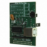
Manufacturer Part Number
MCP6S22DM-PICTL
Description
BOARD DEMO FOR MCP6S22
Manufacturer
Microchip Technology
Series
PICtail™r
Specifications of MCP6S22DM-PICTL
Channels Per Ic
2 - Dual
Amplifier Type
Programmable Gain
Output Type
Single-Ended, Rail-to-Rail
Slew Rate
22 V/µs
-3db Bandwidth
12MHz
Current - Output / Channel
30mA
Operating Temperature
-40°C ~ 85°C
Current - Supply (main Ic)
1mA
Voltage - Supply, Single/dual (±)
2.5 V ~ 5.5 V
Board Type
Fully Populated
Utilized Ic / Part
MCP6S22
Lead Free Status / RoHS Status
Contains lead / RoHS non-compliant
Available stocks
Company
Part Number
Manufacturer
Quantity
Price

Part Number:
MCP6S22DM-PICTL
Manufacturer:
MICROCHIP/微芯
Quantity:
20 000


MCP6S21/2/6/8
1.0
Absolute Maximum Ratings †
V
All inputs and outputs....................... V
Difference Input voltage ........................................ |V
Output Short Circuit Current...................................continuous
Current at Input Pin
Current at Output and Supply Pins
Storage temperature .....................................-65°C to +150°C
Junction temperature .................................................. +150°C
ESD protection on all pins (HBM;MM)
† Notice: Stresses above those listed under "Maximum
Ratings" may cause permanent damage to the device. This is
a stress rating only and functional operation of the device at
those or any other conditions above those indicated in the
operation listings of this specification is not implied. Exposure
to maximum rating conditions for extended periods may affect
device reliability.
DC CHARACTERISTICS
DS21117A-page 2
Electrical Specifications: Unless otherwise indicated, T
Input = CH0 = (0.3V)/G, CH1 to CH7 = 0.3V, R
Amplifier Input
Input Offset Voltage
Input Offset Voltage Drift
Power Supply Rejection Ratio
Input Bias Current
Input Bias Current over
Temperature
Input Impedance
Input Voltage Range
Amplifier Gain
Nominal Gains
DC Gain Error
DC Gain Drift
Internal Resistance
Internal Resistance over
Temperature
Amplifier Output
DC Output Non-linearity G = +1
Maximum Output Voltage Swing
Short-Circuit Current
Note 1: R
DD
- V
SS
2: I
3: The output goes Hi-Z and the registers reset to their defaults; see Section 5.4, “Power-On Reset”.
ELECTRICAL
CHARACTERISTICS
.........................................................................7.0V
Parameters
V
recommend the MCP6S22’s V
Q
LAD
REF
includes current in R
(R
tied internally to V
F
+ R
G = +1
G
G = +1
G
G
G
in Figure 4-1) connects V
+2
+2
+2
LAD
SS
V
R
V
PSRR
OH
I
SS
, so V
R
V
V
Sym
G/ T
G/ T
LAD
V
O(SC)
V
OS
Z
(typically 60 µA at V
g
g
G
ONL
ONL
I
I
LAD
IVR
OS
B
B
, V
IN
E
E
- 0.3V to V
/ T
/ T
SS
OL
A
A
SS
A
A
pin be tied directly to ground to avoid noise problems.
is coupled to the internal amplifier and the PSRR spec describes PSRR+ only. We
L
V
V
V
= 10 k to V
SS
SS
SS
-275
2 kV; 200V
Min
-0.1
-1.0
—
3.4
70
—
—
—
—
—
—
—
—
—
—
DD
DD
+20
+60
REF
0.3
30 mA
+0.3V
- V
2 mA
, V
A
SS
10
1 to 32
±0.0002
±0.0004
OUT
= +25°C, V
+0.028
±0.003
±0.001
OUT
|
Typ
±30
13
4.9
DD
±4
85
±1
—
—
—
—
—
—
—
||15
and the inverting input of the internal amplifier. The MCP6S22 has
= 0.3V). Both I
/2, SI and SCK are tied low and CS is tied high.
V
V
DD
V
PIN FUNCTION TABLE
DD
DD
+275
Max
+0.1
+1.0
DD
250
—
6.4
CH0-CH7
—
—
—
—
—
—
—
—
—
—
= +2.5V to +5.5V, V
-100
+0.3
-60
Name
V
V
SCK
V
V
SO
CS
OUT
SI
REF
SS
DD
Q
and I
% of FSR V
% of FSR V
µV/°C
Units
%/°C
%/°C
%/°C
V/V
mV
mA
dB
k
µV
pA
pA
||pF
%
%
V
Q_SHDN
Analog Output
Analog Inputs
Negative Power Supply
Positive Power Supply
SPI Clock Input
SPI Serial Data Input
SPI Serial Data Output
SPI Chip Select
External Reference Pin
+1, +2, +4, +5, +8, +10, +16 or +32
G = +1, V
T
G = +1 (Note 1)
CHx = V
T
CHx = V
V
V
T
T
(Note 1)
(Note 1)
T
G
G
V
SS
exclude digital switching currents.
A
A
A
A
A
OUT
OUT
OUT
OUT
REF
= -40 to +85°C
= -40 to +85°C,
= -40 to +85°C
= -40 to +85°C
= -40 to +85°C
= GND, V
+2; 0.5V output overdrive
+2; 0.5V output overdrive,
= V
= 0.3V to V
= 0.3V to V
2003 Microchip Technology Inc.
0.3V to V
0.3V to V
DD
DD
DD
DD
/2
/2
Function
/2
= 4.0V
REF
Conditions
DD
DD
DD
DD
= V
SS
0.3V, V
0.3V, V
0.3V
0.3V
, G = +1 V/V,
DD
DD
= 5.0V
= 5.0V
Related parts for MCP6S22DM-PICTL
Image
Part Number
Description
Manufacturer
Datasheet
Request
R

Part Number:
Description:
Manufacturer:
Microchip Technology Inc.
Datasheet:
Part Number:
Description:
Manufacturer:
Microchip Technology Inc.
Datasheet:
Part Number:
Description:
Manufacturer:
Microchip Technology Inc.
Datasheet:
Part Number:
Description:
Manufacturer:
Microchip Technology Inc.
Datasheet:
Part Number:
Description:
Manufacturer:
Microchip Technology Inc.
Datasheet:
Part Number:
Description:
Manufacturer:
Microchip Technology Inc.
Datasheet:
Part Number:
Description:
Manufacturer:
Microchip Technology Inc.
Datasheet:
Part Number:
Description:
Manufacturer:
Microchip Technology Inc.
Datasheet: