LP38512MR-ADJEV/NOPB National Semiconductor, LP38512MR-ADJEV/NOPB Datasheet - Page 3
LP38512MR-ADJEV/NOPB
Manufacturer Part Number
LP38512MR-ADJEV/NOPB
Description
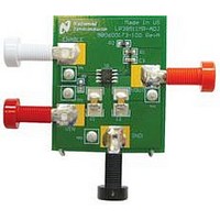
BOARD EVALUATION FOR LP38512
Manufacturer
National Semiconductor
Datasheets
1.LP38512MR-ADJEVNOPB.pdf
(14 pages)
2.LP38512MR-ADJEVNOPB.pdf
(8 pages)
3.LP38512MR-ADJEVNOPB.pdf
(14 pages)
Specifications of LP38512MR-ADJEV/NOPB
Channels Per Ic
1 - Single
Voltage - Output
1.2V
Current - Output
1.5A
Voltage - Input
2.25 ~ 5.5V
Regulator Type
Positive Adjustable
Operating Temperature
-40°C ~ 125°C
Board Type
Fully Populated
Utilized Ic / Part
LP38512
Silicon Manufacturer
National
Silicon Core Number
LP38512MR-ADJ
Kit Application Type
Power Management - Voltage Regulator
Application Sub Type
LDO
Kit Contents
Board, Doc
Lead Free Status / RoHS Status
Contains lead / RoHS non-compliant
Other names
LP38512MR-ADJEV


Enable Input
ΔV
ΔV
Absolute Maximum Ratings
If Military/Aerospace specified devices are required,
please contact the National Semiconductor Sales Office/
Distributors for availability and specifications.
Electrical Characteristics
Unless otherwise specified: V
25°C only; limits in boldface type apply over the junction temperature (T
limits are guaranteed through test, design, or statistical correlation. Typical values represent the most likely parametric norm at
T
Storage Temperature Range
Soldering Temperature (Note 3)
ESD Rating (Note 2)
Power Dissipation(Note 4)
Input Pin Voltage (Survival)
Enable Pin Voltage (Survival)
Output Pin Voltage (Survival)
ERROR Pin Voltage (Survival)
I
V
Symbol
V
J
OUT
V
OUT
OUT
t
EN(OFF)
EN(HYS)
t
V
= 25°C, and are provided for reference purposes only.
d(OFF)
TO-220, Wave
TO-263
I
EN(ON)
V
d(ON)
GND
I
I
OUT
SC
EN
DO
(Survival)
/ΔI
/ΔV
OUT
IN
Output Voltage Tolerance
(Note 7)
Output Voltage Line
Regulation
(Notes 5, 7)
Output Voltage Load
Regulation
(Notes 6, 7)
Dropout Voltage
(Note 8)
Ground Pin Current, Output
Enabled
Ground Pin Current, Output
Disabled
Short Circuit Current
Enable ON Threshold
Enable OFF Threshold
Enable Hysteresis
Turn-off delay
Turn-on delay
Enable Pin Current
Parameter
IN
= 2.5V, I
OUT
−65°C to +150°C
Internally Limited
Internally Limited
−0.3V to +6.0V
−0.3V to +6.0V
−0.3V to +6.0V
= 10 mA, C
2.25V
10 mA
2.25V
10 mA
I
I
ERROR pin = GND
I
ERROR pin = GND
V
ERROR pin = GND
V
V
V
V
V
V
Time from V
OFF, I
Time from V
ON, I
V
V
0.3V to +6.0V
OUT
OUT
OUT
EN
OUT
EN
OUT
EN
OUT
EN(ON)
EN
EN
(Note 1)
260°C, 10s
235°C, 30s
= 0.50V
rising from 0.50V until
falling from 1.60V until
= V
= 0V
= 1.5A
= 10 mA
= 1.5A
LOAD
= 0V
= ON
= OFF
≤
≤
LOAD
≤
≤
- V
IN
±2 kV
V
V
I
I
OUT
OUT
IN
IN
IN
= 1.5A
EN(OFF)
Conditions
= 1.5A
EN
EN
= 10 µF, C
≤
≤
≤
≤
5.5V
5.5V
< V
>V
1.5A
1.5A
EN(ON)
3
EN(OFF)
Operating Ratings
OUT
Input Supply Voltage, V
Enable Input Voltage, V
ERROR Pin Voltage
Output Current (DC)
Junction Temperature (Note 4)
to V
to V
= 10 µF, V
J
) range of -40°C to +125°C. Minimum and Maximum
OUT
OUT
=
=
EN
−2.5
0.90
0.80
0.60
0.50
Min
-1.0
= V
-
-
-
-
-
-
-
-
-
-
-
-
IN
. Limits in standard type are for T
IN
EN
0.02
0.06
0.25
0.40
1.20
1.00
Typ
250
200
7.5
9.5
0.1
2.5
25
-1
0
1
1
(Note 1)
Max
+1.0
+2.5
1.50
1.60
1.40
1.50
340
400
−40°C to +125°C
3.5
11
12
13
14
12
-
-
-
-
-
-
-
-
2.25V to 5.5V
0 mA to 1.5A
0.0V to 5.5V
www.national.com
0.0V to V
Units
%/V
%/A
mV
mA
mV
µA
nA
µs
%
A
V
J
=
IN
Related parts for LP38512MR-ADJEV/NOPB
Image
Part Number
Description
Manufacturer
Datasheet
Request
R

Part Number:
Description:
IC REG LDO 1.5A ADJ 8-PSOP
Manufacturer:
National Semiconductor
Datasheet:

Part Number:
Description:
National Semiconductor [8-Bit D/A Converter]
Manufacturer:
National Semiconductor
Datasheet:
Part Number:
Description:
National Semiconductor [Media Coprocessor]
Manufacturer:
National Semiconductor
Datasheet:
Part Number:
Description:
Digitally Controlled Tone and Volume Circuit with Stereo Audio Power Amplifier, Microphone Preamp Stage and National 3D Sound
Manufacturer:
National Semiconductor
Datasheet:
Part Number:
Description:
Digitally Controlled Tone and Volume Circuit with Stereo Audio Power Amplifier, Microphone Preamp Stage and National 3D Sound
Manufacturer:
National Semiconductor
Datasheet:
Part Number:
Description:
AC97 Rev 2 Codec with Sample Rate Conversion and National 3D Sound
Manufacturer:
National Semiconductor
Part Number:
Description:
Manufacturer:
National Semiconductor
Datasheet:
Part Number:
Description:
Manufacturer:
National Semiconductor
Datasheet:
Part Number:
Description:
General Purpose, Low Voltage, Low Power, Rail-to-Rail Output Operational Amplifiers
Manufacturer:
National Semiconductor
Datasheet:
Part Number:
Description:
8-bit 20 MSPS flash A/D converter.
Manufacturer:
National Semiconductor
Datasheet:
Part Number:
Description:
Low Noise Quad Operational Amplifier
Manufacturer:
National Semiconductor
Datasheet:
Part Number:
Description:
Quad Differential Line Receivers
Manufacturer:
National Semiconductor
Datasheet:
Part Number:
Description:
Quad High Speed Trapezoidal? Bus Transceiver
Manufacturer:
National Semiconductor
Datasheet:
Part Number:
Description:
Dual Line Receiver
Manufacturer:
National Semiconductor
Datasheet: