NCP565VADJEVB ON Semiconductor, NCP565VADJEVB Datasheet - Page 4
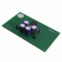
NCP565VADJEVB
Manufacturer Part Number
NCP565VADJEVB
Description
EVAL BOARD FOR NCP565VADJ
Manufacturer
ON Semiconductor
Specifications of NCP565VADJEVB
Design Resources
NCP565 ADJ Demo Board BOM NCP565VADJEVB Gerber Files NCP565 ADJ Demo Board Schematic
Channels Per Ic
1 - Single
Voltage - Output
3.3V
Current - Output
1.5A
Voltage - Input
5V
Regulator Type
Positive Fixed
Board Type
Fully Populated
Utilized Ic / Part
NCP565
Lead Free Status / RoHS Status
Lead free / RoHS Compliant
Operating Temperature
-
Lead Free Status / Rohs Status
Lead free / RoHS Compliant
For Use With/related Products
NCP565VADJ
Other names
NCP565VADJEVBOS


4. Performance guaranteed over specified operating conditions by design, guard banded test limits, and/or characterization, production tested at
5. Typical values are based on design and/or characterization.
6. Dropout voltage is a measurement of the minimum input/output differential at full load.
ELECTRICAL CHARACTERISTICS
ADJUSTABLE OUTPUT VERSION
FIXED OUTPUT VOLTAGE (V
Reference Voltage (10 mA < I
Reference Voltage (10 mA < I
ADJ Pin Current (Note 5)
Line Regulation (I
Load Regulation (10 mA < I
Dropout Voltage (I
Current Limit
Ripple Rejection (120 Hz; I
Ripple Rejection (1 kHz; I
Ground Current (I
Output Noise Voltage (f = 100 Hz to 100 kHz, I
Thermal Shutdown Protection (Note 5)
Output Voltage (10 mA < I
Output Voltage (10 mA < I
Output Voltage (10 mA < I
Output Voltage (10 mA < I
Output Voltage (10 mA < I
Output Voltage (10 mA < I
Output Voltage (10 mA < I
Output Voltage (10 mA < I
Output Voltage (10 mA < I
Output Voltage (10 mA < I
Line Regulation (I
Load Regulation (10 mA < I
Dropout Voltage (I
Current Limit
Ripple Rejection (120 Hz; I
Ripple Rejection (1 kHz; I
Ground Current (I
Output Noise Voltage (f = 100 Hz to 100 kHz, V
Thermal Shutdown Protection (Note 5)
T
1.2 V version
1.2 V version
1.5 V version
1.5 V version
2.8 V version
2.8 V version
3.0 V version
3.0 V version
3.3 V version
3.3 V version
J
= T
A
= 25_C. Low duty cycle pulse techniques are used during testing to maintain the junction temperature as close to ambient as possible.
out
out
out
out
out
out
= 10 mA) (Note 5)
= 1.5 A)
= 10 mA) (Note 5)
= 1.5 A)
= 1.5 A, V
= 1.5 A, V
out
out
out
out
out
out
out
out
out
out
out
out
out
out
out
out
= 1.5 A) (Note 5)
= 1.5 A) (Note 5)
< 1.5 A; 2.8 V < V
< 1.5 A; 2.8 V < V
< 1.5 A; 3.1 V < V
< 1.5 A; 3.1 V < V
< 1.5 A; 4.4 V < V
< 1.5 A; 4.4 V < V
< 1.5 A; 4.6 V < V
< 1.5 A; 4.6 V < V
< 1.5 A; 4.9 V < V
< 1.5 A; 4.9 V < V
out
out
= 1.5 A) (Note 5)
= 1.5 A) (Note 5)
in
< 1.5 A) (Note 5)
< 1.5 A) (Note 5)
out
out
= V
< 1.5 A; V
< 1.5 A; V
= 2.5 V) (Note 6)
= 2.5 V) (Note 6)
Characteristic
out
+ 1.6 V, T
(V
out
out
in
= V
+ 1.6 V < V
+ 1.6 V < V
out
in
in
in
in
in
in
in
in
out
in
in
A
out
< 9.0 V; T
< 9.0 V; T
< 9.0 V; T
< 9.0 V; T
< 9.0 V; T
< 9.0 V; T
< 9.0 V; T
< 9.0 V; T
= 1.5 A) (Note 5)
< 9.0 V; T
< 9.0 V; T
= 25°C, C
= 1.2 V, I
+ 1.6 V, V
in
in
http://onsemi.com
A
A
A
A
A
A
A
A
< 9.0 V; T
< 9.0 V; T
A
A
out
in
= −10 to 105°C)
= −40 to 125°C)
= −10 to 105°C)
= −40 to 125°C)
= −10 to 105°C)
= −40 to 125°C)
= −10 to 105°C)
= −40 to 125°C)
= −10 to 105°C)
= −40 to 125°C)
out
= C
= 1.5 A) (Note 5)
= 0.9 V, T
out
4
A
A
= 150 mF, unless otherwise noted, Note 4.)
= −10 to 105°C)
= −40 to 125°C)
A
= 25°C, C
in
= C
Symbol
Reg
Reg
Reg
Reg
T
T
out
I
I
Vdo
V
V
V
V
V
V
V
V
V
V
Vdo
V
V
I
RR
RR
GND
RR
RR
GND
I
I
V
SHD
V
SHD
Adj
lim
lim
out
out
out
out
out
out
out
out
out
out
ref
ref
load
n
load
n
= 150 mF, unless otherwise noted, Note 4.)
line
line
(−2%)
(−3%)
(−2%)
(−3%)
(−2%)
(−3%)
(−2%)
(−3%)
(−2%)
(−3%)
(−2%)
(−3%)
0.882
0.873
1.176
1.164
1.470
1.455
2.744
2.716
2.940
2.910
3.234
3.201
Min
1.6
1.6
−
−
−
−
−
−
−
−
−
−
−
−
−
−
−
−
−
0.03
0.03
0.03
0.03
Typ
160
160
0.9
0.9
0.9
3.3
1.5
1.2
1.2
1.5
1.5
2.8
2.8
3.0
3.0
3.3
3.3
0.9
3.3
1.5
30
85
75
28
85
75
38
(+2%)
(+3%)
(+2%)
(+3%)
(+2%)
(+3%)
(+2%)
(+3%)
(+2%)
(+3%)
(+2%)
(+3%)
0.918
0.927
1.224
1.236
1.530
1.545
2.856
2.884
3.060
3.090
3.366
3.399
Max
1.3
3.0
1.3
3.0
−
−
−
−
−
−
−
−
−
−
−
−
−
−
−
mVrms
mVrms
Unit
mA
mA
nA
dB
dB
_C
dB
dB
_C
%
%
%
%
V
V
V
A
V
V
V
V
V
V
V
V
V
V
V
A
Related parts for NCP565VADJEVB
Image
Part Number
Description
Manufacturer
Datasheet
Request
R

Part Number:
Description:
ON Semiconductor [VOLTAGE REGULATOR]
Manufacturer:
ON Semiconductor
Datasheet:
Part Number:
Description:
357-036-542-201 CARDEDGE 36POS DL .156 BLK LOPRO
Manufacturer:
ON Semiconductor
Datasheet:
Part Number:
Description:
357-036-542-201 CARDEDGE 36POS DL .156 BLK LOPRO
Manufacturer:
ON Semiconductor
Datasheet:
Part Number:
Description:
357-036-542-201 CARDEDGE 36POS DL .156 BLK LOPRO
Manufacturer:
ON Semiconductor
Datasheet:
Part Number:
Description:
357-036-542-201 CARDEDGE 36POS DL .156 BLK LOPRO
Manufacturer:
ON Semiconductor
Datasheet:
Part Number:
Description:
357-036-542-201 CARDEDGE 36POS DL .156 BLK LOPRO
Manufacturer:
ON Semiconductor
Datasheet:
Part Number:
Description:
357-036-542-201 CARDEDGE 36POS DL .156 BLK LOPRO
Manufacturer:
ON Semiconductor
Datasheet:
Part Number:
Description:
357-036-542-201 CARDEDGE 36POS DL .156 BLK LOPRO
Manufacturer:
ON Semiconductor
Datasheet:
Part Number:
Description:
357-036-542-201 CARDEDGE 36POS DL .156 BLK LOPRO
Manufacturer:
ON Semiconductor
Datasheet:
Part Number:
Description:
357-036-542-201 CARDEDGE 36POS DL .156 BLK LOPRO
Manufacturer:
ON Semiconductor
Datasheet:
Part Number:
Description:
357-036-542-201 CARDEDGE 36POS DL .156 BLK LOPRO
Manufacturer:
ON Semiconductor
Datasheet:
Part Number:
Description:
Manufacturer:
ON Semiconductor
Datasheet:
Part Number:
Description:
Manufacturer:
ON Semiconductor
Datasheet:
Part Number:
Description:
Manufacturer:
ON Semiconductor
Datasheet: