NCP565VADJEVB ON Semiconductor, NCP565VADJEVB Datasheet - Page 2
NCP565VADJEVB
Manufacturer Part Number
NCP565VADJEVB
Description
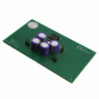
EVAL BOARD FOR NCP565VADJ
Manufacturer
ON Semiconductor
Specifications of NCP565VADJEVB
Design Resources
NCP565 ADJ Demo Board BOM NCP565VADJEVB Gerber Files NCP565 ADJ Demo Board Schematic
Channels Per Ic
1 - Single
Voltage - Output
3.3V
Current - Output
1.5A
Voltage - Input
5V
Regulator Type
Positive Fixed
Board Type
Fully Populated
Utilized Ic / Part
NCP565
Lead Free Status / RoHS Status
Lead free / RoHS Compliant
Operating Temperature
-
Lead Free Status / Rohs Status
Lead free / RoHS Compliant
For Use With/related Products
NCP565VADJ
Other names
NCP565VADJEVBOS


V
PIN DESCRIPTION
Adj. Version
in
Vin
D
Pin No.
3, Tab
Cin
2
PAK 5
1
2
4
5
Figure 1. Typical Application Schematic,
Reference
Voltage
Block
Figure 3. Block Diagram, Fixed Output
V
ref
Fixed Version
= 0.9 V
Vin
D
Pin No.
Shutdown
2, Tab
Thermal
2
PAK 3
Block
−
1
3
−
Fixed Output
NCP565
GND
GND
Output
Stage
Adj. Version
Vout
Pin No.
1, 2
3
6
4
5
DFN6
Current
Sense
Fixed Version
Limit
Cout
Pin No.
1, 2, 5
Vout
3
6
4
−
http://onsemi.com
Vout
Vin
Fixed Version
2
Cin
SOT−223
Pin No.
2, Tab
Vin
−
3
1
−
Figure 2. Typical Application Schematic,
Figure 4. Block Diagram, Adjustable Output
Reference
Voltage
Block
Vin
Symbol
Ground
V
N.C.
V
Adj
V
ref
Adjustable Output
out
in
NCP565
= 0.9 V
GND
Shutdown
Thermal
Block
−
Positive Power Supply Input Voltage
Power Supply Ground
Regulated Output Voltage
This pin is to be connected to the sense
resistors on the output. The linear
regulator will attempt to maintain 0.9 V
between this pin and ground. Refer to
the Application Information section for
output voltage setting.
Vout
ADJ
Output
Stage
GND
Description
5.6 pF
C1
Current
Sense
Limit
R1
R2
Cout
Vout
ADJ
Vout
Related parts for NCP565VADJEVB
Image
Part Number
Description
Manufacturer
Datasheet
Request
R

Part Number:
Description:
ON Semiconductor [VOLTAGE REGULATOR]
Manufacturer:
ON Semiconductor
Datasheet:
Part Number:
Description:
357-036-542-201 CARDEDGE 36POS DL .156 BLK LOPRO
Manufacturer:
ON Semiconductor
Datasheet:
Part Number:
Description:
357-036-542-201 CARDEDGE 36POS DL .156 BLK LOPRO
Manufacturer:
ON Semiconductor
Datasheet:
Part Number:
Description:
357-036-542-201 CARDEDGE 36POS DL .156 BLK LOPRO
Manufacturer:
ON Semiconductor
Datasheet:
Part Number:
Description:
357-036-542-201 CARDEDGE 36POS DL .156 BLK LOPRO
Manufacturer:
ON Semiconductor
Datasheet:
Part Number:
Description:
357-036-542-201 CARDEDGE 36POS DL .156 BLK LOPRO
Manufacturer:
ON Semiconductor
Datasheet:
Part Number:
Description:
357-036-542-201 CARDEDGE 36POS DL .156 BLK LOPRO
Manufacturer:
ON Semiconductor
Datasheet:
Part Number:
Description:
357-036-542-201 CARDEDGE 36POS DL .156 BLK LOPRO
Manufacturer:
ON Semiconductor
Datasheet:
Part Number:
Description:
357-036-542-201 CARDEDGE 36POS DL .156 BLK LOPRO
Manufacturer:
ON Semiconductor
Datasheet:
Part Number:
Description:
357-036-542-201 CARDEDGE 36POS DL .156 BLK LOPRO
Manufacturer:
ON Semiconductor
Datasheet:
Part Number:
Description:
357-036-542-201 CARDEDGE 36POS DL .156 BLK LOPRO
Manufacturer:
ON Semiconductor
Datasheet:
Part Number:
Description:
Manufacturer:
ON Semiconductor
Datasheet:
Part Number:
Description:
Manufacturer:
ON Semiconductor
Datasheet:
Part Number:
Description:
Manufacturer:
ON Semiconductor
Datasheet: