LP3943ISQEV/NOPB National Semiconductor, LP3943ISQEV/NOPB Datasheet - Page 5
LP3943ISQEV/NOPB
Manufacturer Part Number
LP3943ISQEV/NOPB
Description
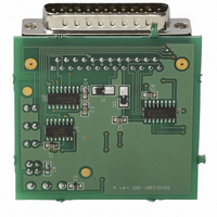
BOARD EVAL FOR LP3943 FUNLIGHT
Manufacturer
National Semiconductor
Series
PowerWise®r
Specifications of LP3943ISQEV/NOPB
Current - Output / Channel
25mA
Outputs And Type
16, Non-Isolated
Voltage - Output
4 V
Features
Dimmable
Voltage - Input
2.3 ~ 5.5 V
Utilized Ic / Part
LP3943
Lead Free Status / RoHS Status
Lead free / RoHS Compliant
Other names
*LP3943ISQEV
*LP3943ISQEV/NOPB
LP3943ISQEV
*LP3943ISQEV/NOPB
LP3943ISQEV


I
t
t
t
t
t
t
2
CLK-HP
SU
DATA-HOLD
DATA-SU
SU
TRANS
Symbol
Electrical Characteristics
Unless otherwise noted, V
in boldface type apply over the entire junction temperature range for operation, T
Note 1: Absolute Maximum Ratings are limits beyond which damage to the device may occur. Operating Ratings are conditions under which operation of the device
is guaranteed. Operating Ratings do not imply guaranteed performance limits. For guaranteed performance limits and associated test conditions, see the Electrical
Characteristics tables.
Note 2: All voltages are with respect to the potential at the GND pin.
Note 3: The part cannot dissipate more than 400mW.
Note 4: The human-body model is 100 pF discharged through 1.5 kΩ. The machine model is 0Ω in series with 100 pF.
Note 5: Limits are guaranteed. All electrical characteristics having room-temperature limits are tested during production with T
guaranteed by correlating the electrical characteristics to process and temperature variations and applying statistical process control.
Note 6: Each LED pin should not exceed 25 mA and each octal (LED0–LED7; LED8–LED15) should not exceed 100 mA. The package should not exceed a total
of 200 mA.
Note 7: Guaranteed by design.
Typical Performance Characteristics
C INTERFACE (SCL AND SDA PINS)
CLK High Period
Set-Up Time Repeated
START Condition
Data Hold Time
Data Set-Up Time
Set-Up Time for STOP
Condition
Maximum Pulse Width of
Spikes that Must Be
Suppressed by the Input
Filter of Both DATA & CLK
Signals
Parameter
DD
= 5.5V. Typical values and limits appearing in normal type apply for T
(Continued)
(Note 7)
(Note 7)
(Note 7)
(Note 7)
(Note 7)
(Note 7)
(T
Frequency vs. Temp
Conditions
V
A
DD
= −40˚C to +85˚C),
= 2.3V to 3.0V
5
Typical
20079617
50
J
= −40˚C to +125˚C. (Note 5)
Min
300
100
0.6
0.6
0.6
J
J
= 25˚C. All hot and cold limits are
Limit
= 25˚C. Limits appearing
Max
www.national.com
Units
µs
µs
ns
ns
µs
ns
Related parts for LP3943ISQEV/NOPB
Image
Part Number
Description
Manufacturer
Datasheet
Request
R

Part Number:
Description:
LED Driver IC
Manufacturer:
National Semiconductor
Datasheet:

Part Number:
Description:
IC LED DRIVER RGB 24-LLP
Manufacturer:
National Semiconductor
Datasheet:

Part Number:
Description:
National Semiconductor [8-Bit D/A Converter]
Manufacturer:
National Semiconductor
Datasheet:
Part Number:
Description:
National Semiconductor [Media Coprocessor]
Manufacturer:
National Semiconductor
Datasheet:
Part Number:
Description:
Digitally Controlled Tone and Volume Circuit with Stereo Audio Power Amplifier, Microphone Preamp Stage and National 3D Sound
Manufacturer:
National Semiconductor
Datasheet:
Part Number:
Description:
Digitally Controlled Tone and Volume Circuit with Stereo Audio Power Amplifier, Microphone Preamp Stage and National 3D Sound
Manufacturer:
National Semiconductor
Datasheet:
Part Number:
Description:
AC97 Rev 2 Codec with Sample Rate Conversion and National 3D Sound
Manufacturer:
National Semiconductor
Part Number:
Description:
Manufacturer:
National Semiconductor
Datasheet:
Part Number:
Description:
Manufacturer:
National Semiconductor
Datasheet:
Part Number:
Description:
General Purpose, Low Voltage, Low Power, Rail-to-Rail Output Operational Amplifiers
Manufacturer:
National Semiconductor
Datasheet:
Part Number:
Description:
8-bit 20 MSPS flash A/D converter.
Manufacturer:
National Semiconductor
Datasheet:
Part Number:
Description:
Low Noise Quad Operational Amplifier
Manufacturer:
National Semiconductor
Datasheet:
Part Number:
Description:
Quad Differential Line Receivers
Manufacturer:
National Semiconductor
Datasheet:
Part Number:
Description:
Quad High Speed Trapezoidal? Bus Transceiver
Manufacturer:
National Semiconductor
Datasheet: