LM3405XEVAL National Semiconductor, LM3405XEVAL Datasheet - Page 12
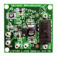
LM3405XEVAL
Manufacturer Part Number
LM3405XEVAL
Description
BOARD EVALUATION LM3405X
Manufacturer
National Semiconductor
Series
PowerWise®r
Specifications of LM3405XEVAL
Current - Output / Channel
1A
Outputs And Type
1, Non-Isolated
Voltage - Output
0.2 ~ 13.5 V
Features
Dimmable
Voltage - Input
3 ~ 15V
Utilized Ic / Part
LM3405
Kit Contents
Board, Datasheet
Svhc
No SVHC (15-Dec-2010)
Kit Features
Cycle-by-Cycle Current Limit,
Rohs Compliant
No
Lead Free Status / RoHS Status
Contains lead / RoHS non-compliant


www.national.com
BOOST CAPACITOR (C3)
A 0.01µF ceramic capacitor with a voltage rating of at least
6.3V is sufficient. The X7R and X5R MLCCs provide the best
performance.
POWER LOSS ESTIMATION
The main power loss in LM3405 includes three basic types of
loss in the internal power switch: conduction loss, switching
loss, and gate charge loss. In addition, there is loss associ-
ated with the power required for the internal circuitry of IC.
The conduction loss is calculated as:
If the inductor ripple current is fairly small (for example, less
than 40%) , the conduction loss can be simplified to:
The switching loss occurs during the switch on and off tran-
sition periods, where voltage and current overlap resulting in
power loss. The simplest means to determine this loss is to
empirically measure the rise and fall times (10% to 90%) of
the voltage at the switch pin.
Switching power loss is calculated as follows:
The gate charge loss is associated with the gate charge Q
required to drive the switch:
The power loss required for operation of the internal circuitry:
I
1.8mA for the LM3405.
The total power loss in the IC is:
An example of power losses for a typical application is shown
in Table 2:
Q
D is calculated to be 0.37
is the quiescent operating current, and is typically around
R
T
T
V
DS(ON)
I
V
f
V
Q
OUT
RISE
FALL
OUT
SW
I
D1
Q
IN
G
P
Σ ( P
SW
Conditions
P
TABLE 2. Power Loss Tabulation
= 0.5 x V
INTERNAL
COND
P
COND
1.6MHz
300mΩ
1.8mA
0.45V
1.4nC
+ P
P
P
4.1V
1.0A
18ns
12ns
12V
INTERNAL
G
= P
IN
SW
= f
P
= I
x I
Q
COND
SW
F
+ P
F
= I
2
x f
x R
x V
Q
Q
= 448mW
SW
+ P
x V
+ P
IN
DS(ON)
x ( T
SW
P
IN
x Q
G
P
COND
P
P
SW
) = P
+ P
Q
G
G
RISE
x D
Power loss
G
INTERNAL
+ T
+ P
FALL
Q
111mW
288mW
22mW
27mW
)
G
12
PCB Layout Considerations
When planning layout there are a few things to consider when
trying to achieve a clean, regulated output. The most impor-
tant consideration when completing the layout is the close
coupling of the GND connections of the input capacitor C1
and the catch diode D1. These ground ends should be close
to one another and be connected to the GND plane with at
least two through-holes. Place these components as close to
the IC as possible. The next consideration is the location of
the GND connection of the output capacitor C2, which should
be near the GND connections of C1 and D1.
There should be a continuous ground plane on the bottom
layer of a two-layer board except under the switching node
island.
The FB pin is a high impedance node and care should be
taken to make the FB trace short to avoid noise pickup that
causes inaccurate regulation. The LED current setting resis-
tor R1 should be placed as close as possible to the IC, with
the GND of R1 placed as close as possible to the GND of the
IC. The V
the inductor and any other traces that are switching.
High AC currents flow through the V
so they should be as short and wide as possible. Radiated
noise can be decreased by choosing a shielded inductor.
The remaining components should also be placed as close
as possible to the IC. Please see Application Note AN-1229
for further considerations and the LM3405 demo board as an
example of a four-layer layout.
OUT
trace to LED anode should be routed away from
IN
, SW and V
OUT
traces,
Related parts for LM3405XEVAL
Image
Part Number
Description
Manufacturer
Datasheet
Request
R

Part Number:
Description:
Precision Fahrenheit Temperature Sensors
Manufacturer:
National Semiconductor
Part Number:
Description:
National Semiconductor [8-Bit D/A Converter]
Manufacturer:
National Semiconductor
Datasheet:
Part Number:
Description:
National Semiconductor [Media Coprocessor]
Manufacturer:
National Semiconductor
Datasheet:
Part Number:
Description:
Digitally Controlled Tone and Volume Circuit with Stereo Audio Power Amplifier, Microphone Preamp Stage and National 3D Sound
Manufacturer:
National Semiconductor
Datasheet:
Part Number:
Description:
Digitally Controlled Tone and Volume Circuit with Stereo Audio Power Amplifier, Microphone Preamp Stage and National 3D Sound
Manufacturer:
National Semiconductor
Datasheet:
Part Number:
Description:
AC97 Rev 2 Codec with Sample Rate Conversion and National 3D Sound
Manufacturer:
National Semiconductor
Part Number:
Description:
Manufacturer:
National Semiconductor
Datasheet:
Part Number:
Description:
Manufacturer:
National Semiconductor
Datasheet:
Part Number:
Description:
General Purpose, Low Voltage, Low Power, Rail-to-Rail Output Operational Amplifiers
Manufacturer:
National Semiconductor
Datasheet:
Part Number:
Description:
8-bit 20 MSPS flash A/D converter.
Manufacturer:
National Semiconductor
Datasheet:
Part Number:
Description:
Low Noise Quad Operational Amplifier
Manufacturer:
National Semiconductor
Datasheet:
Part Number:
Description:
Quad Differential Line Receivers
Manufacturer:
National Semiconductor
Datasheet:
Part Number:
Description:
Quad High Speed Trapezoidal? Bus Transceiver
Manufacturer:
National Semiconductor
Datasheet: