IRPLLED1 International Rectifier, IRPLLED1 Datasheet - Page 23
IRPLLED1
Manufacturer Part Number
IRPLLED1
Description
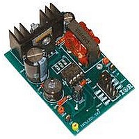
BOARD EVALUATION FOR IRS2540PBF
Manufacturer
International Rectifier
Specifications of IRPLLED1
Current - Output / Channel
1.5A
Outputs And Type
1, Non-Isolated
Voltage - Output
24V
Features
Dimmable
Voltage - Input
50 ~ 170V
Utilized Ic / Part
IRS2540PBF
Core Chip
IRS2540, IRS2541, IRS25401
Topology
Buck (Step Down)
No. Of Outputs
1
Output Current
1.5A
Output Voltage
500mV
Dimming Control Type
PWM
Development Tool Type
Hardware - Eval/Demo Board
Lead Free Status / RoHS Status
Contains lead / RoHS compliant by exemption


The open load protection circuit in Fig 29 is recommended for isolated non-dimming applications where the load
may be disconnected and then reconnected without shutting down the driver. When the load is reconnected with
power on this would reduce the initial surge of current to the output reducing stress on the LEDs .
Connecting the over voltage protection network to the IFB pin instead of the ENN pin in dimming systems is
possible, however since this can introduce noise into the sensitive IFB pin, this is not recommended.
In an open circuit condition, switching will continue at the HO and LO outputs, whether due to the output voltage
clamp or to the watchdog timer. In this state using the protection circuit of Fig 29, rather than regulating the current
with the feedback pin the output voltage will be loosely regulated via the enable pin. Transients and switching will
be observed at the positive output terminal as seen in Fig. 30. The difference in signal shape, between the output
voltage and the IFB, is due to the capacitor CEN used to form the voltage clamp. The repetition of the spikes can be
reduced by simply increasing the cap size. If VBUS is significantly larger than the desired output voltage clamp, the
output voltage will become a function of VBUS. This is because of the intrinsic delays of the chip (t_LO_on,
t_LO_off, t_HO_on, and t_HO_off) along with the minimum HO on time. If the load is removed, the output will
clamp at the desired voltage. Then if the bus voltage is increased there could be a proportional change in the
clamped voltage.
Fig. 30 Open Circuit Fault Signals, with Clamp
The two resistors ROV1 and ROV2 form a voltage divider for the output, which is then fed into the cathode of the
zener diode DOV. The diode will only conduct, flooding the enable pin, when its nominal voltage is exceeded. The
chip will enter a disabled state once the divider network produces a voltage at least 2.5V greater than the zener
rating. The capacitor CEN serves only to filter and slow the transients/switching at the positive output terminal.
The clamped output voltage can be determined by the following analysis.
(
)(
)
+
+
2
5 .
V
DZ
R
R
=
1
2
V
out
R
2
=
Zener
Diode
Nominal
Rated
Voltage
DZ
DOV has been chosen to be a 7.5V zener diode. ROV2 has also been set to 390Ω to help provide a low resistive
charging path for CBOOT as previously discussed. It was also decided to clamp the output voltage at 30V, this is
sufficiently larger than the predefined maximum load voltage of 24V as to not cause any erroneous shut-down,
while it is also well within the specifications of the 100V rated output stage. Having arbitrarily chosen these
parameters, ROV1 was calculated as follows:
RD-0608
23
www.irf.com
Related parts for IRPLLED1
Image
Part Number
Description
Manufacturer
Datasheet
Request
R

Part Number:
Description:
SCHOTTKY RECTIFIER
Manufacturer:
International Rectifier Corp.
Datasheet:
Part Number:
Description:
SCHOTTKY RECTIFIER
Manufacturer:
International Rectifier Corp.
Datasheet:
Part Number:
Description:
SCHOTTKY RECTIFIER
Manufacturer:
International Rectifier Corp.
Datasheet:
Part Number:
Description:
SCHOTTKY RECTIFIER
Manufacturer:
International Rectifier Corp.
Datasheet:
Part Number:
Description:
SCHOTTKY RECTIFIER
Manufacturer:
International Rectifier Corp.
Datasheet:
Part Number:
Description:
SCHOTTKY RECTIFIER
Manufacturer:
International Rectifier Corp.
Datasheet:
Part Number:
Description:
SCHOTTKY RECTIFIER
Manufacturer:
International Rectifier Corp.
Datasheet:
Part Number:
Description:
SCHOTTKY RECTIFIER
Manufacturer:
International Rectifier Corp.
Datasheet:
Part Number:
Description:
SCHOTTKY RECTIFIER
Manufacturer:
International Rectifier Corp.
Datasheet:
Part Number:
Description:
SCHOTTKY RECTIFIER
Manufacturer:
International Rectifier Corp.
Datasheet:
Part Number:
Description:
SCHOTTKY RECTIFIER
Manufacturer:
International Rectifier Corp.
Datasheet:
Part Number:
Description:
SCHOTTKY RECTIFIER
Manufacturer:
International Rectifier Corp.
Datasheet:
Part Number:
Description:
SCHOTTKY RECTIFIER
Manufacturer:
International Rectifier Corp.
Datasheet:
Part Number:
Description:
SCHOTTKY RECTIFIER
Manufacturer:
International Rectifier Corp.
Datasheet:
Part Number:
Description:
SCHOTTKY RECTIFIER
Manufacturer:
International Rectifier Corp.
Datasheet: