IRPLLED1 International Rectifier, IRPLLED1 Datasheet - Page 12
IRPLLED1
Manufacturer Part Number
IRPLLED1
Description
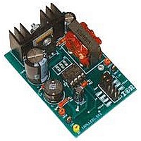
BOARD EVALUATION FOR IRS2540PBF
Manufacturer
International Rectifier
Specifications of IRPLLED1
Current - Output / Channel
1.5A
Outputs And Type
1, Non-Isolated
Voltage - Output
24V
Features
Dimmable
Voltage - Input
50 ~ 170V
Utilized Ic / Part
IRS2540PBF
Core Chip
IRS2540, IRS2541, IRS25401
Topology
Buck (Step Down)
No. Of Outputs
1
Output Current
1.5A
Output Voltage
500mV
Dimming Control Type
PWM
Development Tool Type
Hardware - Eval/Demo Board
Lead Free Status / RoHS Status
Contains lead / RoHS compliant by exemption


Note: Rout is needed only in few applications
The reverse recovery problem is incurred during the deadtime after the low side MOSFET has been on and
conducting current. During this deadtime the lowside MOSFET is off, but the body diode is freewheeling and
providing current to the load. Since the body diode is conducting current, carriers are present and will eventually
need to be recombined, leading to reverse recovery delay. When the high side MOSFET turns on the VS node is
very rapidly pulled from COM to VBUS and the low side MOSFET or the freewheeling diode conducts current
from VS to ground due to the reverse recovery effect, potentially resulting in large power losses. This can result in
overheating of the low side switching component and component stress, as can be seen in Fig. 17 to 18. Since the
power diode has a much shorter reverse recovery time the diode will conduct current for a significantly shorter
period and exhibit lower power losses. At lower frequency and reduced load current, the long recovery time
associated with the MOSFET body diode may not be an issue. For higher frequency higher current applications a
diode could provide lower power losses with respect to a MOSFET.
In this evaluation board the reverse recovery current peaks using a low side MOSFET could be on the order of 8A,
which puts a lot of stress on the components and creates increased operating temperature. By replacing the low side
MOSFET with an appropriate freewheeling diode the reverse recovery current peaks are reduced and limited to
4.5A. The frequency was also selected to keep the diode reverse recovery associated power losses low.
With the inclusion of a freewheeling diode instead of a lowside MOSFET comes the need for RS3 and DVCC.
Without an initial pulse to come from LO to switch on the lower MOSFET and establish a ground reference for
CBOOT to charge, an alternative means of charging CBOOT must be established. RS3 allows this charging path to
exist without any interference from the chip Vcc, likewise DVCC also allows this path to remain isolated. As the
bus voltage is increased, the path will allow CBOOT to fully charge and remain charged until the chip comes out of
UVLO. At which time the self powering feature will take over after the first pulse from HO and the ground
reference will then be created by the freewheeling diode.
www.irf.com
VBUS
COM
Fig. 16 Alternate IRS2540/1 Time-Delayed Hysteretic Controlled Evaluation Board Schematic
EN
L 2
CBUS1
CBUS2
ROV
ROV 2
DPWR
CEN1
DCLAMP
DEN 1
CEN2
DOV
RS2
CVCC 1
RSYNC
CVCC 2
RD-0608
CF
RS 1
COM
VCC
ENN
IFB
1
2
3
4
DBOOT
DSYNC
IC 1
RF
8
7
6
5
VS
LO
HO
VB
RS 3
CBOOT
RG 1
D 1
M1
JDIM
REG
L 1
COUT
ROUT
DIM
RCS6
RCS2
RCS4
RCS7
RCS8
RCS3
RCS5
RCS1
JSET
VOUT
VOUT +
12
Related parts for IRPLLED1
Image
Part Number
Description
Manufacturer
Datasheet
Request
R

Part Number:
Description:
SCHOTTKY RECTIFIER
Manufacturer:
International Rectifier Corp.
Datasheet:
Part Number:
Description:
SCHOTTKY RECTIFIER
Manufacturer:
International Rectifier Corp.
Datasheet:
Part Number:
Description:
SCHOTTKY RECTIFIER
Manufacturer:
International Rectifier Corp.
Datasheet:
Part Number:
Description:
SCHOTTKY RECTIFIER
Manufacturer:
International Rectifier Corp.
Datasheet:
Part Number:
Description:
SCHOTTKY RECTIFIER
Manufacturer:
International Rectifier Corp.
Datasheet:
Part Number:
Description:
SCHOTTKY RECTIFIER
Manufacturer:
International Rectifier Corp.
Datasheet:
Part Number:
Description:
SCHOTTKY RECTIFIER
Manufacturer:
International Rectifier Corp.
Datasheet:
Part Number:
Description:
SCHOTTKY RECTIFIER
Manufacturer:
International Rectifier Corp.
Datasheet:
Part Number:
Description:
SCHOTTKY RECTIFIER
Manufacturer:
International Rectifier Corp.
Datasheet:
Part Number:
Description:
SCHOTTKY RECTIFIER
Manufacturer:
International Rectifier Corp.
Datasheet:
Part Number:
Description:
SCHOTTKY RECTIFIER
Manufacturer:
International Rectifier Corp.
Datasheet:
Part Number:
Description:
SCHOTTKY RECTIFIER
Manufacturer:
International Rectifier Corp.
Datasheet:
Part Number:
Description:
SCHOTTKY RECTIFIER
Manufacturer:
International Rectifier Corp.
Datasheet:
Part Number:
Description:
SCHOTTKY RECTIFIER
Manufacturer:
International Rectifier Corp.
Datasheet:
Part Number:
Description:
SCHOTTKY RECTIFIER
Manufacturer:
International Rectifier Corp.
Datasheet: