LM3503ITL-25EV National Semiconductor, LM3503ITL-25EV Datasheet - Page 5
LM3503ITL-25EV
Manufacturer Part Number
LM3503ITL-25EV
Description
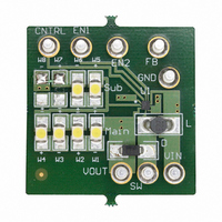
BOARD EVALUATION LM3503ITL-25
Manufacturer
National Semiconductor
Series
PowerWise®r
Specifications of LM3503ITL-25EV
Current - Output / Channel
9mA
Outputs And Type
2, Non-Isolated
Voltage - Output
25 V
Features
Dual Display(s)
Voltage - Input
2.7 ~ 5.5V
Utilized Ic / Part
LM3503
Core Chip
LM3503
Topology
Boost
No. Of Outputs
1
Output Voltage
25V
Input Voltage
2.5V To 5.5V
Development Tool Type
Hardware - Eval/Demo Board
Lead Free Status / RoHS Status
Not applicable / Not applicable


V
I
V
I
I
F
R
R
R
D
I
I
I
Q
CL
Fb
Sw
V OUT1(OFF)
V OUT1(ON)
Symbol
S
IN
Fb
DS(ON)
PDS(ON)
NDS(ON)
MAX
Absolute Maximum Ratings
If Military/Aerospace specified devices are required,
please contact the National Semiconductor Sales Office/
Distributors for availability and specifications.
Electrical Characteristics
face apply over the full operating junction temperature range (−40˚C ≤ T
V
Sw Pin
Fb Pin
Cntrl Pin
V
V
En1
En2
Continuous Power Dissipation
Maximum Junction Temperature
Storage Temperature Range
IN
OUT1
OUT2
(T
Pin
J-MAX
Pin
Pin
Input Voltage
Non-Switching
Switching
Shutdown
Feedback Voltage
NMOS Power Switch
Current Limit
Feedback Pin Output
Bias Current
Switching Frequency
NMOS Power Switch
ON Resistance
(Figure 1: N1)
PMOS ON Resistance
Of V
Switch (Figure 1: P1)
NMOS ON Resistance
Of V
(Figure 1: N2)
Maximum Duty Cycle
Sw Pin Leakage
Current (Note 3)
V
Current (Note 3)
V
Current (Note 3)
)
OUT1
OUT1
OUT1
OUT2
Parameter
Pin Leakage
Pin Bias
/V
/Fb Switch
OUT2
Cntrl = 1.6V
Fb = 0V, Sw Is Floating
En1 = En2 = 0V
Cntrl = 3.5V
16, Fb = 0V
25, Fb = 0V
35, Fb = 0V
44,FB = 0V
Fb = 0.25V, Cntrl = 1.6V
I
I
I
Fb = 0V
Sw = 42V, En1 = En2 =0V
V
V
V
V
V
V
V
V
Sw
PMOS
NMOS
OUT1
OUT1
OUT1
OUT1
OUT1
OUT1
OUT1
OUT1
= 500 mA, (Note 8)
= 20 mA, En1 = 0V, En2 = 1.5V
= 20 mA, En1 = 1.5V, En2 = 0V
= 14V, En1 = En2 = 0V (16)
= 23V, En1 = En2 = 0V (25)
= 32V, En1 = En2 = 0V (35)
= 42V, En1 = En2 = 0V (44)
= 14V, En1 = En1 = 1.5V (16)
= 23V, En1 = En2 = 1.5V (25)
= 32V, En1 = En2 = 1.5V (35)
= 42V, En1 = En2 = 1.5V (44)
Internally Limited
−65˚C to +150˚C
(Notes 6, 7) Limits in standard typeface are for T
−0.3V to V
−0.3V to +5.5V
−0.3V to +5.5V
−0.3V to +5.5V
−0.3V to +5.5V
−0.3V to +5.5V
−0.3V to +48V
−0.3V to +48V
(Note 1)
+150˚C
Conditions
OUT1
5
Operating Conditions
Thermal Properties
ESD Rating (Note 2)
Junction Temperature (T
Ambient Temperature (T
Supply Voltage, V
En1 and En2 Pins
Cntrl Pin
Junction-to-Ambient Thermal Resistance (θ
Micro SMD Package
Leadless Leadframe Package
Human Body Model:
Machine Model:
J
≤ +125˚C). Unless otherwise specified,V
IN
Min
250
400
450
450
2.5
0.5
0.8
90
Pin
A
J
) Range
) Range
J
= +25˚C. Limits in bold type-
0.55
0.55
0.01
Typ
400
600
750
750
0.5
1.9
0.1
2.5
0.1
0.1
0.1
0.1
64
95
40
50
50
85
1
5
(Note 4)
(Notes 1, 6)
1050
1050
Max
650
800
500
100
100
140
5.5
0.6
1.2
1.1
10
80
−40˚C to +125˚C
1
3
3
5
5
3
3
3
3
−40˚C to +85˚C
JA
)
2.5V to 5.5V
IN
www.national.com
0V to 5.5V
0V to 3.5V
= 2.5V.
65˚C/W
49˚C/W
Units
MHz
mA
mA
mA
µA
nA
µA
µA
µA
200V
%
Ω
Ω
Ω
V
V
2 kV
Related parts for LM3503ITL-25EV
Image
Part Number
Description
Manufacturer
Datasheet
Request
R

Part Number:
Description:
IC LED DRVR WHT BCKLT 10MICROSMD
Manufacturer:
National Semiconductor
Datasheet:
Part Number:
Description:
IC LED DRVR WHT BCKLT 10MICROSMD
Manufacturer:
National Semiconductor
Datasheet:
Part Number:
Description:
IC LED DRVR WHT BCKLT 10MICROSMD
Manufacturer:
National Semiconductor
Datasheet:
Part Number:
Description:
IC LED DRVR WHT BCKLT 10MICROSMD
Manufacturer:
National Semiconductor
Datasheet:

Part Number:
Description:
IC, LED DRIVER, CONSTANT CURRENT, µSMD16
Manufacturer:
National Semiconductor
Datasheet:

Part Number:
Description:
Dual-Display Constant Current LED Driver with Analog Brightness Control
Manufacturer:
National Semiconductor
Datasheet:
Part Number:
Description:
LM3503 Dual-Display Constant Current LED Driver with Analog Brightness Control; Package: MICRO SMD; No of Pins: 10; Qty per Container: 250; Container: Reel
Manufacturer:
National Semiconductor
Datasheet:
Part Number:
Description:
National Semiconductor [8-Bit D/A Converter]
Manufacturer:
National Semiconductor
Datasheet:
Part Number:
Description:
National Semiconductor [Media Coprocessor]
Manufacturer:
National Semiconductor
Datasheet:
Part Number:
Description:
Digitally Controlled Tone and Volume Circuit with Stereo Audio Power Amplifier, Microphone Preamp Stage and National 3D Sound
Manufacturer:
National Semiconductor
Datasheet:
Part Number:
Description:
Digitally Controlled Tone and Volume Circuit with Stereo Audio Power Amplifier, Microphone Preamp Stage and National 3D Sound
Manufacturer:
National Semiconductor
Datasheet:
Part Number:
Description:
AC97 Rev 2 Codec with Sample Rate Conversion and National 3D Sound
Manufacturer:
National Semiconductor
Part Number:
Description:
Manufacturer:
National Semiconductor
Datasheet:
Part Number:
Description:
Manufacturer:
National Semiconductor
Datasheet: