LM2793LDEV National Semiconductor, LM2793LDEV Datasheet - Page 9
LM2793LDEV
Manufacturer Part Number
LM2793LDEV
Description
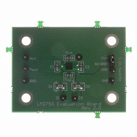
BOARD EVALUATION LM2793LD
Manufacturer
National Semiconductor
Series
PowerWise®r
Specifications of LM2793LDEV
Current - Output / Channel
16mA
Outputs And Type
2, Non-Isolated
Voltage - Output
4 V
Features
Charge Pump
Voltage - Input
2.7 ~ 5.5V
Utilized Ic / Part
LM2793
Lead Free Status / RoHS Status
Not applicable / Not applicable


Application Information
The junction temperature rating takes precedence over the
ambient temperature rating. The LM2793 may be operated
outside the ambient temperature rating, so long as the junc-
tion temperature of the device does not exceed the maxi-
mum operating rating of 100˚C. The maximum ambient tem-
perature rating must be derated in applications where high
power dissipation and/or poor thermal resistance causes the
junction temperature to exceed 100˚C.
PCB Layout Considerations
The LLP is a leadframe based Chip Scale Package (CSP)
with very good thermal properties. This package has an
exposed DAP (die attach pad) at the center of the package
= 85˚C + (0.149W x 55˚C/W)
T
J
= T
A
+ (P
= 93˚C
DMAX
x θ
JA
)
(Continued)
9
measuring 2.0mm x 1.2mm. The main advantage of this
exposed DAP is to offer lower thermal resistance when it is
soldered to the thermal land on the PCB. For PCB layout,
National highly recommends a 1:1 ratio between the pack-
age and the PCB thermal land. To further enhance thermal
conductivity, the PCB thermal land may include vias to a
ground plane. For more detailed instructions on mounting
LLP packages, please refer to National Semiconductor Ap-
plication Note AN-1187.
www.national.com
Related parts for LM2793LDEV
Image
Part Number
Description
Manufacturer
Datasheet
Request
R

Part Number:
Description:
Accurate, 120 C-150 C Factory Preset Thermostat Lm27 Form
Manufacturer:
National Semiconductor Corporation
Datasheet:

Part Number:
Description:
Factory Preset Thermostat
Manufacturer:
National Semiconductor
Datasheet:
Part Number:
Description:
National Semiconductor [8-Bit D/A Converter]
Manufacturer:
National Semiconductor
Datasheet:
Part Number:
Description:
National Semiconductor [Media Coprocessor]
Manufacturer:
National Semiconductor
Datasheet:
Part Number:
Description:
Digitally Controlled Tone and Volume Circuit with Stereo Audio Power Amplifier, Microphone Preamp Stage and National 3D Sound
Manufacturer:
National Semiconductor
Datasheet:
Part Number:
Description:
Digitally Controlled Tone and Volume Circuit with Stereo Audio Power Amplifier, Microphone Preamp Stage and National 3D Sound
Manufacturer:
National Semiconductor
Datasheet:
Part Number:
Description:
AC97 Rev 2 Codec with Sample Rate Conversion and National 3D Sound
Manufacturer:
National Semiconductor
Part Number:
Description:
Manufacturer:
National Semiconductor
Datasheet:
Part Number:
Description:
Manufacturer:
National Semiconductor
Datasheet:
Part Number:
Description:
General Purpose, Low Voltage, Low Power, Rail-to-Rail Output Operational Amplifiers
Manufacturer:
National Semiconductor
Datasheet:
Part Number:
Description:
8-bit 20 MSPS flash A/D converter.
Manufacturer:
National Semiconductor
Datasheet:
Part Number:
Description:
Low Noise Quad Operational Amplifier
Manufacturer:
National Semiconductor
Datasheet:
Part Number:
Description:
Quad Differential Line Receivers
Manufacturer:
National Semiconductor
Datasheet:
Part Number:
Description:
Quad High Speed Trapezoidal? Bus Transceiver
Manufacturer:
National Semiconductor
Datasheet: