AD9717-EBZ Analog Devices Inc, AD9717-EBZ Datasheet - Page 34
AD9717-EBZ
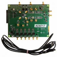
Manufacturer Part Number
AD9717-EBZ
Description
BOARD EVAL FOR AD9717
Manufacturer
Analog Devices Inc
Series
TxDAC®r
Datasheet
1.AD9717BCPZ.pdf
(80 pages)
Specifications of AD9717-EBZ
Number Of Dac's
2
Number Of Bits
14
Outputs And Type
2, Differential
Sampling Rate (per Second)
125M
Data Interface
Serial
Dac Type
Current
Voltage Supply Source
Analog and Digital
Operating Temperature
-40°C ~ 85°C
Utilized Ic / Part
AD9717
Lead Free Status / RoHS Status
Lead free / RoHS Compliant


AD9714/AD9715/AD9716/AD9717
MSB/LSB TRANSFERS
The serial port of the AD9714/AD9715/AD9716/AD9717 can
support both most significant bit (MSB) first or least significant
bit (LSB) first data formats. This functionality is controlled by
the LSBFIRST bit (Register 0x00, Bit 6). The default is MSB first
(LSBFIRST = 0).
When LSBFIRST = 0 (MSB first), the instruction and data bytes
must be written from the most significant bit to the least significant
bit. Multibyte data transfers in MSB first format start with an
instruction byte that includes the register address of the most
significant data byte. Subsequent data bytes should follow in
order from a high address to a low address. In MSB first mode,
the serial port internal byte address generator decrements for
each data byte of the multibyte communications cycle.
When LSBFIRST = 1 (LSB first), the instruction and data bytes
must be written from the least significant bit to the most signifi-
cant bit. Multibyte data transfers in LSB first format start with
an instruction byte that includes the register address of the least
significant data byte followed by multiple data bytes. The serial
port internal byte address generator increments for each byte
of the multibyte communication cycle.
The serial port controller data address of the AD9714/AD9715/
AD9716/AD9717 decrements from the data address written
toward 0x00 for multibyte I/O operations if the MSB first mode
is active. The serial port controller address increments from the
data address written toward 0x1F for multibyte I/O operations
if the LSB first mode is active.
SERIAL PORT OPERATION
The serial port configuration of the AD9714/AD9715/AD9716/
AD9717 is controlled by Register 0x00. It is important to note
that the configuration changes immediately upon writing to the
last bit of the register. For multibyte transfers, writing to this
register can occur during the middle of the communications
cycle. Care must be taken to compensate for this new configu-
ration for the remaining bytes of the current communications cycle.
The same considerations apply to setting the software reset bit
(Register 0x00, Bit 5). All registers are set to their default values
except Register 0x00, which remains unchanged.
Use of single-byte transfers or initiating a software reset is
recommended when changing serial port configurations to
prevent unexpected device behavior.
SCLK
SDIO
CS
Figure 85. Serial Register Interface Timing, MSB First Write
R/W N1 N0 A4 A3
INSTRUCTION CYCLE
A2 A1 A0 D7
N
DATA TRANSFER CYCLE
D6
N
D5
N
D3
0
D2
0
D1
0
D0
0
Rev. A | Page 34 of 80
PIN MODE
The AD9714/AD9715/AD9716/AD9717 can also be operated
without ever writing to the serial port. With the RESET/PINMD
pin tied high, the SCLK pin becomes CLKMD to provide for
clock mode control (see the Retimer section), the SDIO pin
becomes FORMAT and selects the input data format, and the
CS /PWRDN pin serves to power down the device.
Operation is otherwise exactly as defined by the default register
values in Table 13; therefore, external resistors at FSADJI and
FSADJQ are needed to set the DAC currents, and both DACs
are active. This is also a convenient quick checkout mode.
DAC currents can be externally adjusted in pin mode by sourcing
or sinking currents at the FSADJI/AUXI and FSADJQ/AUXQ
pins as desired with the fixed resistors installed. An op amp
output with appropriate series resistance is one of many possibili-
ties. This has the same effect as changing the resistor value.
Place at least 10 kΩ resistors in series right at the DAC to guard
against accidental short circuits and noise modulation. The
REFIO pin can be adjusted ±25% in a similar manner, if desired.
SCLK
SCLK
SCLK
SDIO
SDO
SDIO
SDIO
SDO
CS
CS
CS
Figure 86. Serial Register Interface Timing, MSB First Read
Figure 87. Serial Register Interface Timing, LSB First Write
Figure 88. Serial Register Interface Timing, LSB First Read
R/W N1 N0 A4 A3
A0 A1 A2 A3
A0
INSTRUCTION CYCLE
INSTRUCTION CYCLE
INSTRUCTION CYCLE
A1 A2 A3 A4 N0
A4
N0
A2 A1 A0
N1 R/W
N1 R/W D0
D0
D7
0
D1
D6
DATA TRANSFER CYCLE
DATA TRANSFER CYCLE
DATA TRANSFER CYCLE
D1
0
N
0
D2
D5
D2
0
N
0
D4
D3
D4
N
0
N
D5
D2
D5
N
0
N
D6
D1
D6
N
0
N
D7
D0
D7
N
0
N
Related parts for AD9717-EBZ
Image
Part Number
Description
Manufacturer
Datasheet
Request
R

Part Number:
Description:
Dual 14B, Low Power D-A Converter
Manufacturer:
Analog Devices Inc
Datasheet:

Part Number:
Description:
±1.7g Dual-Axis IMEMS Accelerometer Evaluation Board
Manufacturer:
Analog Devices Inc
Datasheet:
Part Number:
Description:
Inertial Sensor Evaluation System
Manufacturer:
Analog Devices Inc
Datasheet:
Part Number:
Description:
Manufacturer:
Analog Devices Inc
Datasheet:
Part Number:
Description:
Manufacturer:
Analog Devices Inc
Datasheet:
Part Number:
Description:
Manufacturer:
Analog Devices Inc
Datasheet:
Part Number:
Description:
Manufacturer:
Analog Devices Inc
Datasheet:
Part Number:
Description:
Manufacturer:
Analog Devices Inc
Datasheet:
Part Number:
Description:
Manufacturer:
Analog Devices Inc
Datasheet:
Part Number:
Description:
Manufacturer:
Analog Devices Inc
Datasheet:
Part Number:
Description:
Manufacturer:
Analog Devices Inc
Datasheet:
Part Number:
Description:
Manufacturer:
Analog Devices Inc
Datasheet:
Part Number:
Description:
Manufacturer:
Analog Devices Inc
Datasheet: