EVAL-AD5391EBZ Analog Devices Inc, EVAL-AD5391EBZ Datasheet - Page 22
EVAL-AD5391EBZ
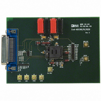
Manufacturer Part Number
EVAL-AD5391EBZ
Description
BOARD EVALUATION FOR AD5391
Manufacturer
Analog Devices Inc
Specifications of EVAL-AD5391EBZ
Number Of Dac's
16
Number Of Bits
12
Outputs And Type
16, Single Ended
Sampling Rate (per Second)
167k
Data Interface
Serial
Settling Time
6µs
Dac Type
Voltage
Voltage Supply Source
Single
Operating Temperature
-40°C ~ 85°C
Utilized Ic / Part
AD5391
Lead Free Status / RoHS Status
Lead free / RoHS Compliant


AD5390/AD5391/AD5392
FUNCTIONAL DESCRIPTION
DAC ARCHITECTURE
The AD5390/AD5391 are complete single-supply, 16-channel,
voltage output DACs offering a resolution of 14 bits and 12 bits,
respectively. The AD5392 is a complete single-supply, 8-channel,
voltage output DAC offering 14-bit resolution. All devices are
available in a 64-lead LFCSP and 52-lead LQFP, and feature
serial interfaces. This family includes an internal select-able
1.25 V/2.5 V, 10 ppm/°C reference that can be used to drive the
buffered reference inputs (alternatively, an external reference
can be used to drive these inputs). All channels have an on-chip
output amplifier with rail-to-rail output capable of driving a
5 kΩ load in parallel with a 200 pF capacitance.
The architecture of a single DAC channel consists of a 12-bit
and 14-bit resistor-string DAC followed by an output buffer
amplifier operating at a gain of 2. This resistor-string architecture
guarantees DAC monotonicity. The 12-bit and 14-bit binary
digital code loaded to the DAC register determines at what
node on the string the voltage is tapped off before being fed to
the output amplifier. Each channel on these devices contains
independent offset and gain control registers, allowing the user
to digitally trim offset and gain.
These registers let the user calibrate out errors in the complete
signal chain including the DAC using the internal m and c
registers, which hold the correction factors. All channels are
double-buffered, allowing synchronous updating of all channels
using the LDAC pin.
single channel on the AD5390/AD5391/AD5392.
INPUT
DATA
x1 INPUT
REG
m REG
c REG
Figure 31. Single-Channel Architecture
x2
Figure 31
DAC
REG
VREF
14-BIT
DAC
shows a block diagram of a
AVDD
R
R
VOUT
Rev. C | Page 22 of 40
The digital input transfer function for each DAC can be
represented as
where:
x 2 is the data-word loaded to the resistor-string DAC.
x 1 is the 12-bit and 14-bit data-word written to the DAC input
register.
m is the 12-bit and 14-bit gain coefficient (default is all 0x3FFE
on the AD5390/AD5392 and 0xFFE on the AD5391). The LSB
of the gain coefficient is zero.
n = DAC resolution ( n = 14 for the AD5390/AD5392 and
n = 12 for the AD5391).
c is the 12-bit and 14-bit offset coefficient (default is 0x2000 on
the AD5390/AD5392 and 0x800 on the AD5391).
The complete transfer function for these devices can be
represented as
where:
x2 is the data-word loaded to the resistor-string DAC.
V
on the DAC when an external reference is used (2.5 V for specified
performance on the AD539x-5 products and 1.25 V on the
AD539x-3 products).
REF
is the reference voltage applied to the REFIN/REFOUT pin
VOUT
x
2
=
(
(
m
=
+
2
2
×
)
VREF
2 /
n
)
×
×
x
1
x
+
2
2 /
(
c
−
n
2
n
−
1
)
Related parts for EVAL-AD5391EBZ
Image
Part Number
Description
Manufacturer
Datasheet
Request
R


Part Number:
Description:
BOARD EVAL FOR SI270X-A
Manufacturer:
Silicon Laboratories Inc
Datasheet:

Part Number:
Description:
BUCK CONV REF DESIGN KIT IP1201
Manufacturer:
International Rectifier
Datasheet:
Part Number:
Description:
BOARD DEMO SYNC DUAL BUCK CNVTER
Manufacturer:
International Rectifier
Datasheet:
Part Number:
Description:
BOARD DEMO SYNC BUCK CONVETER
Manufacturer:
International Rectifier
Datasheet:

Part Number:
Description:
EVALBOARD/EB Omnidirectional microphone - Analog
Manufacturer:
Analog Devices
Datasheet:
Part Number:
Description:
EVALBOARD/EB Omnidirectional microphone - Analog
Manufacturer:
Analog Devices
Datasheet:


Part Number:
Description:
BOARD EVAL LED DRIVER LT3756
Manufacturer:
Linear Technology
Datasheet:

Part Number:
Description:
BOARD EVAL FOR AD7741/7742
Manufacturer:
Analog Devices Inc
Datasheet:

Part Number:
Description:
±1.7g Dual-Axis IMEMS Accelerometer Evaluation Board
Manufacturer:
Analog Devices Inc
Datasheet:

Part Number:
Description:
IC MULTIPLIER ANALOG 8-SOIC T/R
Manufacturer:
Analog Devices Inc
Datasheet:

Part Number:
Description:
IC ANALOG MULTIPLIER 8-DIP
Manufacturer:
Analog Devices Inc
Datasheet:
Part Number:
Description:
IC ANALOG MULTIPLIER 8-SOIC
Manufacturer:
Analog Devices Inc
Datasheet:
Part Number:
Description:
IC ANALOG MULTIPLIER 8-DIP
Manufacturer:
Analog Devices Inc
Datasheet: