EVAL-AD5422EBZ Analog Devices Inc, EVAL-AD5422EBZ Datasheet - Page 3
EVAL-AD5422EBZ
Manufacturer Part Number
EVAL-AD5422EBZ
Description
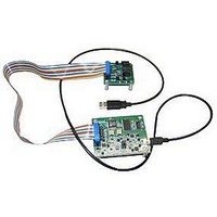
BOARD EVAL FOR AD5422
Manufacturer
Analog Devices Inc
Specifications of EVAL-AD5422EBZ
Number Of Dac's
1
Number Of Bits
16
Outputs And Type
1, Single Ended
Sampling Rate (per Second)
1M
Data Interface
Serial
Settling Time
32µs
Dac Type
Current/Voltage
Voltage Supply Source
Analog and Digital, Dual ±
Operating Temperature
-40°C ~ 85°C
Utilized Ic / Part
AD5422
Silicon Manufacturer
Analog Devices
Application Sub Type
DAC
Kit Application Type
Data Converter
Silicon Core Number
AD5422
Kit Contents
Board And Literature
Lead Free Status / RoHS Status
Lead free / RoHS Compliant


EVALUATION BOARD HARDWARE
POWER SUPPLIES
The following external supplies must be provided:
•
•
•
•
•
The analog and digital planes are connected at one location, close
to the AD5422. It is recommended not to connect GND and
DGND elsewhere in the system to avoid ground loop problems.
Each supply is decoupled to the relevant ground plane with 10 μF
and 0.1 μF capacitors. Each device supply pin is again decoupled
with a 10 μF and 0.1 μF capacitor pair to the relevant ground plane.
Excessive Power Supply
If a power supply in excess of +16.5 V is to be connected to
the AV
damage to the 5 V voltage reference or to the ADC (see U2 and
U6, respectively, in Figure 5). However, if a power supply in excess
of −16.5 V is to be connected to the AV
in Position B to prevent potential damage to the ADC.
LINK OPTIONS
The position of Link 7 configures the board for either PC
control via the USB port (default setup) or for control by an
external source via J8. The link options on the evaluation board
should be set for the required operating setup before using the
board. The functions of the link options are described in Table 4.
5 V between the 5 V and 0 V inputs for the digital supply
of the AD5422 and digital circuitry. Alternatively, place
Link 6 in Position A to power the digital circuitry from the
USB port (default).
10.8 V to 40 V between the AV
analog supply of the AD5422.
0 V to −26.4 V between the AV
negative analog supply of the AD5422. (This is only required
if a bipolar output voltage range is to be programmed;
otherwise, the negative supply of the AD5422 can be
connected to GND by placing Link 4 in Position A.)
10.8 V to 16.5 V between the V+ and GND inputs for the
analog supply of the
(on-board voltage reference). If the analog supply connected
to the AV
can be powered from this by placing LK9 in Position A,
and the V+ input can be left unconnected.
0 V to −16.5 V between the V− and GND inputs for the
negative analog supply of the AD7321 (on-board ADC). If
the negative analog supply connected to the AV
less than (magnitude) −16.5 V, the AD7321 can be powered
from this by placing LK16 in Position A, and the V− input
can be left unconnected.
DD
input, LK9 must be in Position B to prevent potential
DD
input is less than 16.5 V, the AD7321 and ADR435
AD7321
(on-board ADC) and
DD
SS
and GND inputs for the
and GND inputs for the
SS
input, LK16 must be
SS
ADR435
input is
Rev. 0 | Page 3 of 12
Default Link Option Setup
The default setup is for control by the PC via the USB port. The
default link options are listed in Table 1.
Table 1. Link and Switch Defaults (PC Control)
Link No.
LK1
LK2
LK3
LK4
LK5
LK6
LK7
LK8
LK9
LK10
LK11
LK12
LK13
LK14
LK15
LK16
LK17
LK18
Connector J8 Pin Descriptions
Table 2. Connector J8 Pin Configuration
2
1
1
Table 3. Connector J8 Pin Descriptions
Connector J8 Pin No.
1
2
3
4
5
6
7
8
9
10
LK7 must be in Position B to enable the use of J8.
4
3
Option
A
A
Inserted
B
B
A
A
A
A
Inserted
Inserted
Inserted
Inserted
Inserted
C
A
Inserted
Inserted
6
5
Function
SDO
CLEAR SELECT
DGND
CLEAR
DGND
FAULT
SDIN
DGND
SCLK
LATCH
8
7
EVAL-AD5422
1
10
9
Related parts for EVAL-AD5422EBZ
Image
Part Number
Description
Manufacturer
Datasheet
Request
R


Part Number:
Description:
BOARD EVAL FOR SI270X-A
Manufacturer:
Silicon Laboratories Inc
Datasheet:

Part Number:
Description:
BUCK CONV REF DESIGN KIT IP1201
Manufacturer:
International Rectifier
Datasheet:
Part Number:
Description:
BOARD DEMO SYNC DUAL BUCK CNVTER
Manufacturer:
International Rectifier
Datasheet:
Part Number:
Description:
BOARD DEMO SYNC BUCK CONVETER
Manufacturer:
International Rectifier
Datasheet:

Part Number:
Description:
EVALBOARD/EB Omnidirectional microphone - Analog
Manufacturer:
Analog Devices
Datasheet:
Part Number:
Description:
EVALBOARD/EB Omnidirectional microphone - Analog
Manufacturer:
Analog Devices
Datasheet:


Part Number:
Description:
BOARD EVAL LED DRIVER LT3756
Manufacturer:
Linear Technology
Datasheet:

Part Number:
Description:
BOARD EVAL FOR AD7741/7742
Manufacturer:
Analog Devices Inc
Datasheet:

Part Number:
Description:
±1.7g Dual-Axis IMEMS Accelerometer Evaluation Board
Manufacturer:
Analog Devices Inc
Datasheet:

Part Number:
Description:
IC MULTIPLIER ANALOG 8-SOIC T/R
Manufacturer:
Analog Devices Inc
Datasheet:

Part Number:
Description:
IC ANALOG MULTIPLIER 8-DIP
Manufacturer:
Analog Devices Inc
Datasheet:
Part Number:
Description:
IC ANALOG MULTIPLIER 8-SOIC
Manufacturer:
Analog Devices Inc
Datasheet:
Part Number:
Description:
IC ANALOG MULTIPLIER 8-DIP
Manufacturer:
Analog Devices Inc
Datasheet: