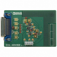
EVAL-AD5415EBZ Analog Devices Inc, EVAL-AD5415EBZ Datasheet - Page 20
EVAL-AD5415EBZ
Manufacturer Part Number
EVAL-AD5415EBZ
Description
BOARD EVALUATION FOR AD5415
Manufacturer
Analog Devices Inc
Specifications of EVAL-AD5415EBZ
Number Of Dac's
2
Number Of Bits
12
Outputs And Type
2, Differential
Sampling Rate (per Second)
2.47M
Data Interface
Serial
Settling Time
120ns
Dac Type
Current
Voltage Supply Source
Single
Operating Temperature
-40°C ~ 125°C
Utilized Ic / Part
AD5415
Lead Free Status / RoHS Status
Lead free / RoHS Compliant


AD5415
SERIAL INTERFACE
The AD5415 has an easy to use 3-wire interface that is
compatible with SPI, QSPI, MICROWIRE, and most DSP
interface standards. Data is written to the device in 16-bit
words. Each 16-bit word consists of four control bits and
12 data bits, as shown in Figure 40.
Low Power Serial Interface
To minimize the power consumption of the device, the interface
only powers up fully when the device is being written to, that is,
on the falling edge of SYNC . The SCLK and DIN input buffers
are powered down on the rising edge of SYNC .
DAC Control Bits C3 to C0
Control Bits C3 to C0 allow control of various functions of the
DAC, as shown in Table 11. Default settings of the DAC at
power on are as follows. Data is clocked into the shift register
on falling clock edges, and daisy-chain mode is enabled. The
device powers on with a zero-scale load to the DAC register and
I
features at power on. For example, daisy-chaining can be
disabled when not in use, an active clock edge can be changed
to a rising edge, and DAC output can be cleared to either zero
scale or midscale. The user can also initiate a readback of the
DAC register contents for verification purposes.
Control Register (Control Bits = 1101)
While maintaining software compatibility with single-channel
current output DACs (AD5426/AD5433/AD5443), this DAC
also features additional interface functionality. Simply set the
control bits to 1101 to enter control register mode. Figure 41
shows the contents of the control register, the functions of
which are described in the following sections.
OUT
lines. The DAC control bits allow the user to adjust certain
DB15 (MSB)
DB15 (MSB)
C3
1
CONTROL BITS
CONTROL BITS
C2
1
C1
0
C0
1
SDO1
DB11
SDO2
DB10
Figure 40. 12-Bit Input Shift Register Contents
Figure 41. Control Register Loading Sequence
DSY
DB9
Rev. B | Page 20 of 32
HCLR
DB8
SCLK
DB7
SDO Control (SDO1 and SDO2)
The SDO bits enable the user to control the SDO output driver
strength, disable the SDO output, or configure it as an open-
drain driver. The strength of the SDO driver affects the timing
of t
Table 10. SDO Control Bits
SDO2
0
0
1
1
Daisy-Chain Control (DSY)
DSY enables or disables daisy-chain mode. A 1 enables daisy-
chain mode; a 0 disables it. When disabled, a readback request
is accepted, SDO is automatically enabled, the DAC register
contents of the relevant DAC are clocked out on SDO, and,
when complete, SDO is disabled again.
Hardware CLR Bit (HCLR)
The default setting for the hardware CLR pin is to clear the
registers and DAC output to zero code. A 1 in the HCLR bit
clears the DAC outputs to midscale; a 0 clears them to zero scale.
Active Clock Edge (SCLK)
The default active clock edge is the falling edge. Write a 1 to this
bit to clock data in on the rising edge; write a 0 to clock it in on
the falling edge.
DB6
DATA BITS
X
12
and, when stronger, allows a faster clock cycle to be used.
DB5
X
SDO1
0
1
0
1
DB4
X
DB3
X
Function
Full SDO driver
Weak SDO driver
SDO configured as open drain
Disable SDO output
DB2
X
DB1
X
DB0 (LSB)
DB0 (LSB)
DB0
X
Related parts for EVAL-AD5415EBZ
Image
Part Number
Description
Manufacturer
Datasheet
Request
R


Part Number:
Description:
BOARD EVAL FOR SI270X-A
Manufacturer:
Silicon Laboratories Inc
Datasheet:

Part Number:
Description:
BUCK CONV REF DESIGN KIT IP1201
Manufacturer:
International Rectifier
Datasheet:
Part Number:
Description:
BOARD DEMO SYNC DUAL BUCK CNVTER
Manufacturer:
International Rectifier
Datasheet:
Part Number:
Description:
BOARD DEMO SYNC BUCK CONVETER
Manufacturer:
International Rectifier
Datasheet:

Part Number:
Description:
EVALBOARD/EB Omnidirectional microphone - Analog
Manufacturer:
Analog Devices
Datasheet:
Part Number:
Description:
EVALBOARD/EB Omnidirectional microphone - Analog
Manufacturer:
Analog Devices
Datasheet:


Part Number:
Description:
BOARD EVAL LED DRIVER LT3756
Manufacturer:
Linear Technology
Datasheet:

Part Number:
Description:
BOARD EVAL FOR AD7741/7742
Manufacturer:
Analog Devices Inc
Datasheet:

Part Number:
Description:
±1.7g Dual-Axis IMEMS Accelerometer Evaluation Board
Manufacturer:
Analog Devices Inc
Datasheet:

Part Number:
Description:
IC MULTIPLIER ANALOG 8-SOIC T/R
Manufacturer:
Analog Devices Inc
Datasheet:

Part Number:
Description:
IC ANALOG MULTIPLIER 8-DIP
Manufacturer:
Analog Devices Inc
Datasheet:
Part Number:
Description:
IC ANALOG MULTIPLIER 8-SOIC
Manufacturer:
Analog Devices Inc
Datasheet:
Part Number:
Description:
IC ANALOG MULTIPLIER 8-DIP
Manufacturer:
Analog Devices Inc
Datasheet: