CDB4365 Cirrus Logic Inc, CDB4365 Datasheet - Page 26
CDB4365
Manufacturer Part Number
CDB4365
Description
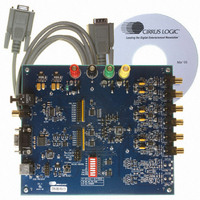
EVALUATION BOARD FOR CS4365
Manufacturer
Cirrus Logic Inc
Specifications of CDB4365
Number Of Dac's
6
Number Of Bits
24
Outputs And Type
6, Differential
Sampling Rate (per Second)
192k
Data Interface
Serial
Dac Type
Voltage
Voltage Supply Source
Analog and Digital
Operating Temperature
-40°C ~ 85°C
Utilized Ic / Part
CS4365
Description/function
Audio D/A
Operating Supply Voltage
5 V
Product
Audio Modules
For Use With/related Products
CS4365
Lead Free Status / RoHS Status
Contains lead / RoHS non-compliant
Lead Free Status / RoHS Status
Lead free / RoHS Compliant, Contains lead / RoHS non-compliant
Other names
598-1779


26
4.7
4.8
ATAPI Specification
The CS4365 implements the channel-mixing functions of the ATAPI CD-ROM specification. The
ATAPI functions are applied per A-B pair. Refer to
tion.
Direct Stream Digital (DSD) Mode
In Software Mode, the DSD/PCM bits (Reg. 02h) are used to configure the device for DSD Mode. The
DSD_DIF bits (Reg 04h) then control the expected DSD rate and MCLK ratio.
The DIR_DSD bit (Reg 04h) selects between two proprietary methods for DSD-to-analog conversion. The
first method uses a decimation-free DSD processing technique which allows for features such as matched
PCM-level output, DSD volume control, and 50kHz on-chip filter. The second method sends the DSD data
directly to the on-chip switched-capacitor filter for conversion (without the above-mentioned features).
The DSD_PM_EN bit (Reg. 04h) selects Phase Modulation (data plus data inverted) as the style of data
input. In this mode, the DSD_PM_mode bit selects whether a 128Fs or 64x clock is used for phase modu-
lated 64x data (see
the CS4365, but may lower the sensitivity to board-level routing of the DSD data signals.
The CS4365 can detect errors in the DSD data which does not comply with the SACD specification. The
STATIC_DSD and INVALID_DSD bits (Reg. 04h) allow the CS4365 to alter the incoming invalid DSD data.
Depending on the error, the data may either be attenuated or replaced with a muted DSD signal (the
MUTEC pins would be set according to the DAMUTE bit (Reg. 08h)).
More information for any of these register bits can be found in
The DSD input structure and analog outputs are designed to handle a nominal 0 dB-SACD (50% modulation
index) at full rated performance. Signals of +3 dB-SACD may be applied for brief periods of time, however;
performance at these levels is not guaranteed. If sustained +3 dB-SACD levels are required, the digital vol-
ume control should be set to -3.0 dB. This same volume control register affects PCM output levels. There
is no need to change the volume control setting between PCM and DSD in order to have the 0dB output
levels match (both 0 dBFS and 0 dB-SACD will output at -3 dB in this case).
SDINx
Right Chan nel
Left Chan nel
Audio D ata
Audio D ata
Figure
Figure 17. ATAPI Block Diagram (x = channel pair 1, 2, or 3)
18). Use of Phase Modulation Mode may not directly affect the performance of
Σ
Table 9 on page 42
A Channel
B Channel
Volume
Volume
Control
Control
Section 7. “Filter Plots” on page
and
Σ
Figure 17
for additional informa-
MUTE
MUTE
Aout Ax
AoutBx
CS4365
45.
DS670F2
Related parts for CDB4365
Image
Part Number
Description
Manufacturer
Datasheet
Request
R

Part Number:
Description:
Development Kit
Manufacturer:
Cirrus Logic Inc
Datasheet:
Part Number:
Description:
Development Kit
Manufacturer:
Cirrus Logic Inc
Datasheet:


Part Number:
Description:
High-efficiency PFC + Fluorescent Lamp Driver Reference Design
Manufacturer:
Cirrus Logic Inc
Datasheet:
Part Number:
Description:
Development Kit
Manufacturer:
Cirrus Logic Inc
Datasheet:
Part Number:
Description:
Development Kit
Manufacturer:
Cirrus Logic Inc
Datasheet:

Part Number:
Description:
Development Kit
Manufacturer:
Cirrus Logic Inc
Datasheet:
Part Number:
Description:
Development Kit
Manufacturer:
Cirrus Logic Inc
Datasheet:
Part Number:
Description:
Development Kit
Manufacturer:
Cirrus Logic Inc
Datasheet:
Part Number:
Description:
Development Kit
Manufacturer:
Cirrus Logic Inc
Datasheet:

Part Number:
Description:
EVALUATION BOARD FOR CS8427
Manufacturer:
Cirrus Logic Inc
Datasheet:

Part Number:
Description:
BOARD EVAL FOR CS8416 RCVR
Manufacturer:
Cirrus Logic Inc
Datasheet:

Part Number:
Description:
EVALUATION BOARD FOR CS8420
Manufacturer:
Cirrus Logic Inc
Datasheet:

Part Number:
Description:
KIT DEVELOPMENT EP9315 ARM9
Manufacturer:
Cirrus Logic Inc
Datasheet:

Part Number:
Description:
KIT DEVELOPMENT EP9302 ARM9
Manufacturer:
Cirrus Logic Inc
Datasheet: