CDB4365 Cirrus Logic Inc, CDB4365 Datasheet
CDB4365
Specifications of CDB4365


Related parts for CDB4365


CDB4365 Summary of contents
Page 1
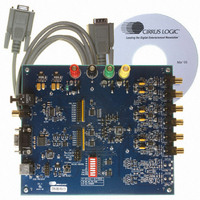
... Inputs for DSD Clocks and Data http://www.cirrus.com Description The CDB4365 evaluation board is an excellent means for quickly evaluating the CS4365 24-bit, 48-pin, 6- channel D/A converter. Evaluation requires an analog signal analyzer, a digital signal source for control- ling the CS4365 (only required for control port mode), and a power supply ...
Page 2
... INPUT FOR CONTROL DATA ............................................................................................................... 4 5. POWER SUPPLY CIRCUITRY ............................................................................................................... 5 6. GROUNDING AND POWER SUPPLY DECOUPLING .......................................................................... 5 7. ANALOG OUTPUT FILTERING ............................................................................................................. 5 8. PERFORMANCE PLOTS ....................................................................................................................... 7 9. CDB4365 SCHEMATICS ..................................................................................................................... 17 10. REVISION HISTORY ......................................................................................................................... 30 LIST OF FIGURES Figure 1.FFT (48 kHz, 0 dB) ....................................................................................................................... 7 Figure 2.FFT (48 kHz, -60 dB) .................................................................................................................... 7 Figure 3.FFT (48 kHz, No Input) ................................................................................................................. 7 Figure 4 ...
Page 3
... Figure 47.Analog Outputs ............................................................................................................ 21 Figure 48.CS8416 S/PDIF Input ............................................................................................................... 22 Figure 49.PCM Input Header and Muxing ................................................................................................. 23 Figure 50.DSD Input Header ..................................................................................................................... 24 Figure 51.Control Input ............................................................................................................................. 25 Figure 52.Power Inputs ............................................................................................................................. 26 Figure 53.Silkscreen Top .......................................................................................................................... 27 Figure 54.Top Side .................................................................................................................................... 28 Figure 55.Bottom Side .............................................................................................................................. 29 LIST OF TABLES Table 1. System Connections .................................................................................................................... 5 Table 2. CDB4365 Jumper Settings ............................................................................................................ 6 DS670DB3 CDB4365 3 ...
Page 4
... The evaluation board also allows the user to supply external PCM or DSD clocks and data through PCB headers for system development. The CDB4365 uses the CDB4385 as a base PCB board. For this reason, there may be additional circuitry on board which is not populated as it has no function for this device. ...
Page 5
... CS4365 as possible. Extensive use of ground plane fill in the evaluation board yields large reductions in radiated noise. 7. ANALOG OUTPUT FILTERING The analog output on the CDB4365 has been designed according to the CS4365 datasheet. This output circuit in- cludes an active 2-pole, 50-kHz filter which uses the multiple-feedback topology. CONNECTOR ...
Page 6
... RX(CS8416), closed = EXT(J11) Selects 128x (open) or 256x (*closed) MCLK/LRCK ratio 7 8 For PCM input set to *Open, for DSD set to Closed *Default Factory Settings Table 2. CDB4365 Jumper Settings CDB4365 FUNCTION SELECTED Reserved for factory use only Default: M0, M4 open (HI) M1, M2, M3 closed (LO) ...
Page 7
... The plots in the following section were acheived using an Audio Precision System 2700 and a randomly chosen pro- duction CDB4365. In some cases the performance may be limited by the CDB4365. All measurements were taken at room temp using the standard AP filter options ( kHz) with default board settings and nominal datasheet voltages applied unless otherwise noted ...
Page 8
... Figure 8. 48 kHz, THD+N vs. Level + -40 -20 +0 Figure 10. 48 kHz, Frequency Response CDB4365 10k 12k 14k 16k 18k Hz Figure 6. FFT (IMD 48 kHz) -80 -60 -40 -20 dBFS 100 200 500 DS670DB3 20k +0 10k 20k ...
Page 9
... Hz Figure 11. 48 kHz, Crosstalk 3 2.5 2 1.5 1 500m V 0 -500m -1 -1 500u 1m 1.5m sec Figure 13. 48 kHz, Impulse Prefilter DS670DB3 3 2.5 2 1.5 1 500m 0 V -500m -1 -1 10k 20k 0 500u Figure 12. 48 kHz, Impulse Response 2m 2.5m 3m CDB4365 1m 1.5m 2m 2.5m 3m sec 9 ...
Page 10
... Hz Figure 15. FFT (96 kHz, 0 dB) 10 Figure 14. 48 kHz Dynamic Range +0 -10 -20 -30 -40 -50 - -70 r -80 A -90 -100 -110 -120 -130 -140 -150 2k 5k 10k 20k 20 50 Figure 16. FFT (96 kHz, -60 dB) CDB4365 100 200 500 10k Hz DS670DB3 20k ...
Page 11
... B - -70 -80 -90 -100 -110 -120 2k 5k 10k 20k -120 Figure 22. 96 kHz, THD+N vs. Level CDB4365 20k 40k 60k 80k 100k 10k 12k 14k 16k Hz Figure 20. FFT (IMD 96 kHz) -100 -80 -60 -40 -20 dBFS 120k 18k 20k +0 11 ...
Page 12
... Figure 27. 96 kHz, Impulse Prefilter -40 -20 +0 Figure 24. 96 kHz, Frequency Response 3 2.5 2 1.5 1 500m 0 V -500m -1 -1 250u 2k 5k 10k 20k Figure 26. 96 kHz, Impulse Response 1m 1.25m 1.5m CDB4365 100 200 500 10k Hz 500u 750u 1m 1.25m sec DS670DB3 20k 1.5m ...
Page 13
... Hz Figure 29. FFT (192 kHz, 0 dB) DS670DB3 Figure 28. Dynamic Range 96 kHz +0 -10 -20 -30 -40 -50 - -70 r -80 A -90 -100 -110 -120 -130 -140 -150 2k 5k 10k 20k 20 50 Figure 30. FFT (192 kHz, -60 dB) CDB4365 100 200 500 10k Hz 20k 13 ...
Page 14
... Figure 34. FFT (IMD 192 kHz) +0 -10 -20 -30 - -70 -80 -90 -100 -110 -120 2k 5k 10k 20k -120 -100 Figure 36. 192 kHz, THD+N vs. Level CDB4365 40k 60k 80k 100k 10k 12k 14k 16k 18k Hz -80 -60 -40 -20 dBFS DS670DB3 120k 20k +0 ...
Page 15
... Figure 41. 192 kHz, Impulse Prefilter DS670DB3 + -40 - Figure 38. 192 kHz, Frequency Response 3 2.5 2 1.5 1 500m 0 V -500m -1 -1 10k 20k Figure 40. 192 kHz, Impulse Response 600u CDB4365 100 200 500 10k Hz 200u 400u 600u sec 20k 15 ...
Page 16
... Figure 42. Dynamic Range 192 kHz CDB4365 DS670DB3 ...
Page 17
... CDB4365 SCHEMATICS PCM HEADER Figure 49 on page 23 PCM Clocks/Data PCM mux PCM Clocks/Data Figure 49 on page 23 CS8416 S/PDIF Input Figure 48 on page 22 Hardware Control Switches Figure 51 on page 25 Serial Control Port Figure 51 on page C/SPI Header CS4365 PCM Clocks/Data DSD clk_enable ...
Page 18
Figure 44. CS4365 ...
Page 19
... DS670DB3 Figure 45. Analog Outputs CDB4365 19 ...
Page 20
... Figure 46. Analog Outputs CDB4365 DS670DB3 ...
Page 21
... Figure 47. Analog Outputs DS670DB3 CDB4365 21 ...
Page 22
Figure 48. CS8416 S/PDIF Input ...
Page 23
Figure 49. PCM Input Header and Muxing ...
Page 24
Figure 50. DSD Input Header ...
Page 25
Figure 51. Control Input ...
Page 26
Figure 52. Power Inputs ...
Page 27
Figure 53. Silkscreen Top ...
Page 28
Figure 54. Top Side ...
Page 29
Figure 55. Bottom Side ...
Page 30
... Cirrus Logic, Cirrus, and the Cirrus Logic logo designs are trademarks of Cirrus Logic, Inc. All other brand and product names in this document may be trademarks or service marks of their respective owners. DSD is a registered trademark of Sony Kabushiki Kaisha TA Sony Company. I² registered trademark of Philips Semiconductor. SPI is a trademark of Motorola, Inc. 30 Changes Section 4. Input for Control Data www.cirrus.com. CDB4365 DS670DB3 ...