CDB4365 Cirrus Logic Inc, CDB4365 Datasheet - Page 5
CDB4365
Manufacturer Part Number
CDB4365
Description
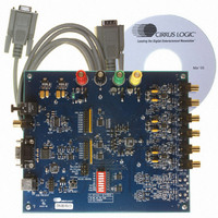
EVALUATION BOARD FOR CS4365
Manufacturer
Cirrus Logic Inc
Specifications of CDB4365
Number Of Dac's
6
Number Of Bits
24
Outputs And Type
6, Differential
Sampling Rate (per Second)
192k
Data Interface
Serial
Dac Type
Voltage
Voltage Supply Source
Analog and Digital
Operating Temperature
-40°C ~ 85°C
Utilized Ic / Part
CS4365
Description/function
Audio D/A
Operating Supply Voltage
5 V
Product
Audio Modules
For Use With/related Products
CS4365
Lead Free Status / RoHS Status
Contains lead / RoHS non-compliant
Lead Free Status / RoHS Status
Lead free / RoHS Compliant, Contains lead / RoHS non-compliant
Other names
598-1779


DS670DB3
source, remove the shunts on J15 and place a ribbon cable so the signal lines are on the center row and the grounds
are on the right side. R116 and R119 should be populated with 2-kΩ resistors when using an external I²C source
that does not already provide pull-ups.
5. POWER SUPPLY CIRCUITRY
Power is supplied to the evaluation board by four binding posts: GND, +5V, +12V, and -12V (See
‘+5V’ terminal supplies VA and the rest of the +5-V circuitry on the board. The +3.3-V circuitry is powered from a
regulator. The +2.5 volts required for VD is also provided from an on-board regulator. The +5-V supply should be
set within the recommended values for VA stated in the CS4365 datasheet.
WARNING: Refer to the CS4365 datasheet for maximum allowable voltage levels. Operation outside this range can
cause permanent damage to the device.
6. GROUNDING AND POWER SUPPLY DECOUPLING
As with any high-performance converter, the CS4365 requires careful attention to power supply and grounding ar-
rangements to optimize performance.
show the component placement and top and bottom layout. The decoupling capacitors are located as close to the
CS4365 as possible. Extensive use of ground plane fill in the evaluation board yields large reductions in radiated
noise.
7. ANALOG OUTPUT FILTERING
The analog output on the CDB4365 has been designed according to the CS4365 datasheet. This output circuit in-
cludes an active 2-pole, 50-kHz filter which uses the multiple-feedback topology.
S/PDIF IN - OPT1
PCM INPUT - J11
DSD INPUT - J7
CONNECTOR
S/PDIF IN - J9
OUTA1-B3
+12V
GND
-12V
+5V
INPUT/OUTPUT
Output
Input
Input
Input
Input
Input
Input
Input
Input
Figure 44
Table 1. System Connections
Digital audio interface input via coax
+ 5 V power
Ground connection from power supply
+12 V positive supply for the on-board filtering
-12 V negative supply for the on-board filtering
Digital audio interface input via optical
Input for master, serial, left/right clocks and serial data
Input for DSD serial clock and DSD data
RCA line level analog outputs
details the connections to the CS4365 and
SIGNAL PRESENT
Figures
Figure
53, 54, and
CDB4365
52). The
55
5
Related parts for CDB4365
Image
Part Number
Description
Manufacturer
Datasheet
Request
R

Part Number:
Description:
Development Kit
Manufacturer:
Cirrus Logic Inc
Datasheet:
Part Number:
Description:
Development Kit
Manufacturer:
Cirrus Logic Inc
Datasheet:


Part Number:
Description:
High-efficiency PFC + Fluorescent Lamp Driver Reference Design
Manufacturer:
Cirrus Logic Inc
Datasheet:
Part Number:
Description:
Development Kit
Manufacturer:
Cirrus Logic Inc
Datasheet:
Part Number:
Description:
Development Kit
Manufacturer:
Cirrus Logic Inc
Datasheet:

Part Number:
Description:
Development Kit
Manufacturer:
Cirrus Logic Inc
Datasheet:
Part Number:
Description:
Development Kit
Manufacturer:
Cirrus Logic Inc
Datasheet:
Part Number:
Description:
Development Kit
Manufacturer:
Cirrus Logic Inc
Datasheet:
Part Number:
Description:
Development Kit
Manufacturer:
Cirrus Logic Inc
Datasheet:

Part Number:
Description:
EVALUATION BOARD FOR CS8427
Manufacturer:
Cirrus Logic Inc
Datasheet:

Part Number:
Description:
BOARD EVAL FOR CS8416 RCVR
Manufacturer:
Cirrus Logic Inc
Datasheet:

Part Number:
Description:
EVALUATION BOARD FOR CS8420
Manufacturer:
Cirrus Logic Inc
Datasheet:

Part Number:
Description:
KIT DEVELOPMENT EP9315 ARM9
Manufacturer:
Cirrus Logic Inc
Datasheet:

Part Number:
Description:
KIT DEVELOPMENT EP9302 ARM9
Manufacturer:
Cirrus Logic Inc
Datasheet: