CDB4353 Cirrus Logic Inc, CDB4353 Datasheet - Page 4
CDB4353
Manufacturer Part Number
CDB4353
Description
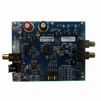
BOARD EVAL FOR CS4353 DAC
Manufacturer
Cirrus Logic Inc
Specifications of CDB4353
Number Of Dac's
2
Number Of Bits
24
Outputs And Type
2, Single Ended
Sampling Rate (per Second)
192k
Data Interface
Serial
Dac Type
Voltage
Voltage Supply Source
Single
Operating Temperature
-40°C ~ 85°C
Utilized Ic / Part
CS4353
Silicon Manufacturer
Cirrus Logic
Application Sub Type
DAC
Kit Application Type
Data Converter
Silicon Core Number
CS4353
Kit Contents
Board
Lead Free Status / RoHS Status
Contains lead / RoHS non-compliant
Lead Free Status / RoHS Status
Contains lead / RoHS non-compliant
Other names
598-1519
CDB-4353
CDB-4353


4
1. CDB4353 SYSTEM OVERVIEW
The CDB4353 evaluation board is an excellent means of quickly evaluating the CS4353. The CS8416 digital audio
interface receiver provides an easy interface to digital audio signal sources, including the majority of digital audio
test equipment. The evaluation board also allows the user to supply external PCM clocks and data through two sep-
arate header options for system development. Configuration of the CDB4353 can be modified through piano switch
S1, see
schematics are shown in
2. CS4353 DIGITAL-to-ANALOG CONVERTER
A description of the CS4353 is included in the CS4353 datasheet.
3. CS8416 DIGITAL AUDIO RECEIVER
The system receives and decodes the standard S/PDIF data format using a CS8416 Digital Audio Receiver,
Figure
clock. The operation of the CS8416 and a discussion of the digital audio interface is included in the CS8416
datasheet.
The evaluation board has been designed such that the input can be either optical or coaxial, see
ever, both inputs cannot be driven simultaneously.
Position 3 of piano switch S1 sets the CS8416 output data format to either I²S (down) or LJ (up). Position 2 of S1
sets the output MCLK to LRCK ratio of the CS8416. This switch should be set to 256 (down) for input Fs<=48 kHz
and can be either 256 (down) or 128 (up) for Fs>48 kHz. The CS8416 must be manually reset via S2 after either
switch has been toggled for the change to take effect.
4. INPUT FOR CLOCKS AND DATA
The evaluation board has been designed to allow interfacing to external systems via headers J13 and J4. Header
J13 allows the evaluation board to accept externally generated PCM clocks and data at a nominal voltage of 3.3 V.
The PCM clocks and data are buffered, level-shifted to the VL supply, and then input to the CS4353. The schematic
for the clock/data input is shown in
(up) or header J13 (down).
Note:
Header J4 bypasses position 1 of S1 and allows for a direct connection of PCM clocks and data to the CS4353.
Under normal operation, shunts placed across the left two rows of J4 connects the PCM clocks and data from the
source specified by position 1 of S1 to the CS4353. An external system can be directly connected to the CS4353 by
removing the shunts on J4 and connecting PCM clocks and data across the right two rows of J4 using a ribbon cable.
A single row of “GND” pins are provided to maintain signal ground integrity. Signals input to header J4 must be at
the same voltage level as the VL supply on the evaluation board. The schematic for the header J4 and CS4353 is
shown in
Please see the CS4353 datasheet for more information on clocking data into the CS4353.
32. The outputs of the CS8416 include a serial bit clock, serial data, left-right clock, and a 128/256 Fs master
If the VL supply is set to a low voltage level (VL<1.8 V), termination resistors may need to be added to the
J13 header signals to match the source and transmission-line impedances that are driving the header. This
may be accomplished by soldering resistors across the rows of J13 on the back of the evaluation board.
Table
Figure
4. The CDB4353 system block diagram and signal flow is shown in
32.
Figures 32
Figure
and 33.
33. Position 1 of S1 selects the CS4353 PCM source as either the CS8416
Figure
31, and the CDB4353
Figure
CDB4353
DS803DB2
32. How-
Related parts for CDB4353
Image
Part Number
Description
Manufacturer
Datasheet
Request
R

Part Number:
Description:
Development Kit
Manufacturer:
Cirrus Logic Inc
Datasheet:
Part Number:
Description:
Development Kit
Manufacturer:
Cirrus Logic Inc
Datasheet:


Part Number:
Description:
High-efficiency PFC + Fluorescent Lamp Driver Reference Design
Manufacturer:
Cirrus Logic Inc
Datasheet:
Part Number:
Description:
Development Kit
Manufacturer:
Cirrus Logic Inc
Datasheet:
Part Number:
Description:
Development Kit
Manufacturer:
Cirrus Logic Inc
Datasheet:

Part Number:
Description:
Development Kit
Manufacturer:
Cirrus Logic Inc
Datasheet:
Part Number:
Description:
Development Kit
Manufacturer:
Cirrus Logic Inc
Datasheet:
Part Number:
Description:
Development Kit
Manufacturer:
Cirrus Logic Inc
Datasheet:
Part Number:
Description:
Development Kit
Manufacturer:
Cirrus Logic Inc
Datasheet:

Part Number:
Description:
EVALUATION BOARD FOR CS8427
Manufacturer:
Cirrus Logic Inc
Datasheet:

Part Number:
Description:
BOARD EVAL FOR CS8416 RCVR
Manufacturer:
Cirrus Logic Inc
Datasheet:

Part Number:
Description:
EVALUATION BOARD FOR CS8420
Manufacturer:
Cirrus Logic Inc
Datasheet:

Part Number:
Description:
KIT DEVELOPMENT EP9315 ARM9
Manufacturer:
Cirrus Logic Inc
Datasheet:

Part Number:
Description:
KIT DEVELOPMENT EP9302 ARM9
Manufacturer:
Cirrus Logic Inc
Datasheet: