MCP4725DM-PTPLS Microchip Technology, MCP4725DM-PTPLS Datasheet - Page 3
MCP4725DM-PTPLS
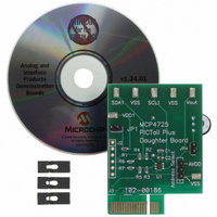
Manufacturer Part Number
MCP4725DM-PTPLS
Description
BOARD DAUGHTER PICTAIL MCP4725
Manufacturer
Microchip Technology
Specifications of MCP4725DM-PTPLS
Number Of Dac's
1
Number Of Bits
12
Outputs And Type
1, Single Ended
Sampling Rate (per Second)
100k ~ 3.4M
Data Interface
I²C
Settling Time
6µs
Dac Type
Voltage
Voltage Supply Source
Single
Operating Temperature
-40°C ~ 125°C
Utilized Ic / Part
MCP4725
Silicon Manufacturer
Microchip
Application Sub Type
DAC
Kit Application Type
Data Converter
Silicon Core Number
MCP4725
Silicon Family Name
PICtail
Lead Free Status / RoHS Status
Lead free / RoHS Compliant
Available stocks
Company
Part Number
Manufacturer
Quantity
Price
Company:

Part Number:
MCP4725DM-PTPLS
Manufacturer:
Microchip Technology
Quantity:
135


1.0
Absolute Maximum Ratings†
V
All inputs and outputs w.r.t V
Current at Input Pins ....................................................±2 mA
Current at Supply Pins ...............................................±50 mA
Current at Output Pins ...............................................±25 mA
Storage Temperature ...................................-65°C to +150°C
Ambient Temp. with Power Applied .............-55°C to +125°C
ESD protection on all pins ................ ≥ 6 kV HBM, ≥ 400V MM
Maximum Junction Temperature (T
ELECTRICAL CHARACTERISTICS
© 2009 Microchip Technology Inc.
Electrical Specifications: Unless otherwise indicated, all parameters apply at
R
Power Requirements
Operating Voltage
Supply Current
Power-Down Current
Power-On-Reset
Threshold Voltage
DC Accuracy
Resolution
INL Error
DNL
Offset Error
Offset Error Drift
Gain Error
Gain Error Drift
Output Amplifier
Phase Margin
Capacitive Load Stability
Slew Rate
Short Circuit Current
Output Voltage Settling
Time
Note 1:
DD
L
...................................................................................6.5V
= 5 kΩ from V
2:
3:
4:
Parameter
ELECTRICAL
CHARACTERISTICS
Test Code Range: 100 to 4000.
This parameter is ensure by design and not 100% tested.
Within 1/2 LSB of the final value when code changes from 1/4 to 3/4 (400h to C00h) of full scale range.
Logic state of external address selection pin (A0 pin).
OUT
to V
SS
SS
.................–0.3V to V
, C
ΔV
ΔG
J
L
V
) ......................... +150°C
Sym
I
DNL
V
V
INL
= 100 pF, T
I
DDP
G
p
SR
I
OS
T
POR
C
DD
SC
DD
n
OS
E
M
S
E
L
/°C
/°C
-0.75
Min
2.7
12
A
—
—
—
—
—
—
—
—
—
—
—
—
-2
= -40°C to +125°C. Typical values are at +25°C.
DD
+0.3V
0.06
±0.2
0.02
0.55
Typ
210
-0.1
±2
±1
±2
66
15
—
—
-3
2
6
† Notice: Stresses above those listed under “Maximum
ratings” may cause permanent damage to the device. This is
a stress rating only and functional operation of the device at
these or any other conditions above those indicated in the
operation listings of this specification is not implied. Exposure
to maximum rating conditions for extended periods may affect
device reliability
±14.5
±0.75
1000
Max
0.75
400
5.5
2.0
24
—
—
—
—
—
—
—
—
2
Degree(°)
% of FSR
% of FSR
ppm/°C
ppm/°C
ppm/°C
Units
LSB
LSB
V/µs
Bits
mA
µA
µA
pF
µs
V
V
V
DD
= + 2.7V to 5.5V,
Digital input pins are
grounded, Output pin (V
is not connected (unloaded),
Code = 000h
V
Code Range = 000h to FFFh
Note 1
Note 1
Code = 000h
-45°C to +25°C
+25°C to +85°C
Code = FFFh,
Offset error is not included.
C
R
V
Note 3
DD
DD
L
L
= 400 pF, R
= 5 kΩ, Note 2
= 5.5V
= 5V, V
MCP4725
Conditions
OUT
DS22039D-page 3
V
L
SS
=
= Grounded
= 0V,
∞
OUT
)
Related parts for MCP4725DM-PTPLS
Image
Part Number
Description
Manufacturer
Datasheet
Request
R

Part Number:
Description:
Manufacturer:
Microchip Technology Inc.
Datasheet:
Part Number:
Description:
Manufacturer:
Microchip Technology Inc.
Datasheet:
Part Number:
Description:
Manufacturer:
Microchip Technology Inc.
Datasheet:
Part Number:
Description:
Manufacturer:
Microchip Technology Inc.
Datasheet:
Part Number:
Description:
Manufacturer:
Microchip Technology Inc.
Datasheet:
Part Number:
Description:
Manufacturer:
Microchip Technology Inc.
Datasheet:
Part Number:
Description:
Manufacturer:
Microchip Technology Inc.
Datasheet:
Part Number:
Description:
Manufacturer:
Microchip Technology Inc.
Datasheet: