MCP4725DM-PTPLS Microchip Technology, MCP4725DM-PTPLS Datasheet - Page 19
MCP4725DM-PTPLS
Manufacturer Part Number
MCP4725DM-PTPLS
Description
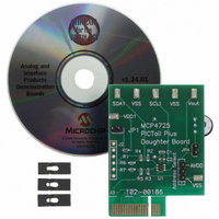
BOARD DAUGHTER PICTAIL MCP4725
Manufacturer
Microchip Technology
Specifications of MCP4725DM-PTPLS
Number Of Dac's
1
Number Of Bits
12
Outputs And Type
1, Single Ended
Sampling Rate (per Second)
100k ~ 3.4M
Data Interface
I²C
Settling Time
6µs
Dac Type
Voltage
Voltage Supply Source
Single
Operating Temperature
-40°C ~ 125°C
Utilized Ic / Part
MCP4725
Silicon Manufacturer
Microchip
Application Sub Type
DAC
Kit Application Type
Data Converter
Silicon Core Number
MCP4725
Silicon Family Name
PICtail
Lead Free Status / RoHS Status
Lead free / RoHS Compliant
Available stocks
Company
Part Number
Manufacturer
Quantity
Price
Company:

Part Number:
MCP4725DM-PTPLS
Manufacturer:
Microchip Technology
Quantity:
135


5.0
The MCP4725 is a single channel buffered voltage
output
(EEPROM). The user can store configuration register
bits (2 bits) and DAC input data (12 bits) in non-volatile
EEPROM (14 bits) memory.
When the device is powered on first, it loads the DAC
code from the EEPROM and outputs the analog output
accordingly with the programmed settings. The user
can reprogram the EEPROM or DAC register any time.
The device uses a resistor string architecture. DAC’s
output is buffered with a low power precision amplifier.
This output amplifier provides low offset voltage and
low noise, as well as rail-to-rail output. The amplifier
can also provide high source currents (V
V
The DAC can be configured to normal or power saving
power-down mode by setting the configuration register
bits.
The device uses a two-wire I
interface and operates from a single power supply
ranging from 2.7V to 5.5V.
5.1
The input coding to the MCP4725 device is unsigned
binary. The output voltage range is from 0V to V
output voltage is given in
EQUATION 5-1:
5.1.1
The DAC output is buffered with a low-power, precision
CMOS amplifier. This amplifier provides low offset
voltage and low noise. The output stage enables the
device to operate with output voltages close to the
power supply rails. Refer to Section 1.0 “Electrical
Characteristics” for range and load conditions.
The output amplifier can drive the resistive and high
capacitive loads without oscillation. The amplifier can
provide maximum load current as high as 25 mA which
is enough for most of a programmable voltage
reference applications.
© 2009 Microchip Technology Inc.
Where:
SS
V
).
REF
D
n
GENERAL DESCRIPTION
12-bit
Output Voltage
=
=
OUTPUT AMPLIFIER
V
V
DAC
Input code
OUT
DD
=
with
Equation
(
------------------------------ -
V
REF
4096
non-volatile
×
2
C compatible serial
D
5-1:
n
)
OUT
memory
DD
pin to
. The
5.1.2
The MCP4725 output stage is capable of driving loads
up to 1000 pF in parallel with 5 kΩ load resistance.
Figure 2-15
drops slowly as the load resistance decreases after
about 3.5 kΩ.
5.2
One LSB is defined as the ideal voltage difference
between two successive codes. (see
Table 5-1
scale range (V
TABLE 5-1:
5.3
The MCP4725 device uses the V
reference. Any variation or noises on the V
affect directly on the DAC output. The V
as clean as possible for accurate DAC performance.
5.4
In the Reset conditions, the device uploads the
EEPROM data into the DAC register. The device can
be reset by two independent events: (a) by POR or (b)
by I
The factory default settings for the EEPROM prior to
shipment are shown in
output). The user can rewrite or read the DAC register
or EEPROM anytime after the Power-On-Reset event.
5.4.1
The device’s internal Power-On-Reset (POR) circuit
ensures that the device powers up in a defined state.
If the power supply voltage is less than the POR thresh-
old (V
there will be no DAC output. When the V
above the V
the reset period, the device uploads all configuration
and DAC input codes from EEPROM. The DAC output
will be the same as for the value last stored in the
EEPROM. This enables the device returns to the same
state that it was at the last write to the EEPROM before
it was powered off.
2
Full Scale
C General Call Reset Command.
Range
POR
(V
3.0V
5.0V
LSB SIZE
DD
Voltage Reference
Reset Conditions
shows an example of the LSB size over full
= 2V, typical), all circuits are disabled and
)
DRIVING RESISTIVE AND
CAPACITIVE LOADS
POWER-ON-RESET
POR
shows the V
DD
, the device takes a reset state. During
).
LSB SIZES FOR MCP4725
(EXAMPLE)
Table 5-3
0.73 mV
1.22 mV
OUT
LSB
Size
vs. Resistive Load. V
MCP4725
(set for a middle scale
DD
DS22039D-page 19
DD
as its voltage
Equation
Condition
3V / 4096
5V / 4096
DD
needs to be
DD
increases
line can
4-1).
OUT
Related parts for MCP4725DM-PTPLS
Image
Part Number
Description
Manufacturer
Datasheet
Request
R

Part Number:
Description:
Manufacturer:
Microchip Technology Inc.
Datasheet:
Part Number:
Description:
Manufacturer:
Microchip Technology Inc.
Datasheet:
Part Number:
Description:
Manufacturer:
Microchip Technology Inc.
Datasheet:
Part Number:
Description:
Manufacturer:
Microchip Technology Inc.
Datasheet:
Part Number:
Description:
Manufacturer:
Microchip Technology Inc.
Datasheet:
Part Number:
Description:
Manufacturer:
Microchip Technology Inc.
Datasheet:
Part Number:
Description:
Manufacturer:
Microchip Technology Inc.
Datasheet:
Part Number:
Description:
Manufacturer:
Microchip Technology Inc.
Datasheet: