LM5088MH-2EVAL National Semiconductor, LM5088MH-2EVAL Datasheet - Page 5
LM5088MH-2EVAL
Manufacturer Part Number
LM5088MH-2EVAL
Description
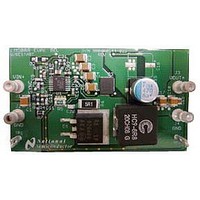
BOARD EVALUATION FOR LM5088MH-2
Manufacturer
National Semiconductor
Series
PowerWise®r
Specifications of LM5088MH-2EVAL
Design Resources
LM(2)5088-1/2 QS Component Calculator
Main Purpose
DC/DC, Step Down
Outputs And Type
1, Non-Isolated
Voltage - Output
5V
Current - Output
7A
Voltage - Input
5.5 ~ 55V
Regulator Topology
Buck
Frequency - Switching
250kHz
Board Type
Fully Populated
Utilized Ic / Part
LM5088
Silicon Manufacturer
National
Silicon Core Number
LM5088
Kit Application Type
Power Management - Voltage Regulator
Application Sub Type
Buck Controller
Kit Contents
Board, Doc
Lead Free Status / RoHS Status
Lead free / RoHS Compliant
Power - Output
-


VIN SUPPLY
VCC REGULATOR
ENABLE THRESHOLDS
SOFT- START
ERROR AMPLIFIER
PWM COMPARATORS
VIN, VOUT to GND
BOOT to GND
SW to GND
VCC to GND
HG to SW
EN to GND
BOOT to SW
I
Absolute Maximum Ratings
If Military/Aerospace specified devices are required,
please contact the National Semiconductor Sales Office/
Distributors for availability and specifications.
Electrical Characteristics
junction temperature (T
correlation. Typical values represent at T
following conditions apply: V
SHUTDOWN
V
V
Symbol
I
V
T
T
STANDBY
VCC(Reg)
VCC(Reg)
HG(OFF)
VCC(UV)
FBW
ON(MIN)
V
AOL
I
BIAS
REF
Parameter
VIN Operating Current
VIN Standby Current
VIN Shutdown Current
VCC Regulation
VCC Regulation
VCC Sourcing Current Limit
VCC Under-Voltage Lockout Threshold Positive going VVCC
VCC Under-Voltage Hysteresis
EN Shutdown Threshold
EN Shutdown Hysteresis
EN Standby Threshold
EN Standby Hysteresis
EN Pull-up Current Source
SS Pull-up Current Source
FB to SS Offset
FB Reference Voltage
FB Input Bias Current
COMP Sink/Source Current
DC Gain
Unity gain bandwidth
Forced HG Off-time
Minimum HG On-time
COMP to PWM comparator offset
J
) range of -40°C to +125°C. Minimum and Maximum limits are guaranteed through test, design, or statistical
VIN
= 48V, V
VCC
J
= 25°C, and are provided for reference purposes only. Unless otherwise stated the
= 8V, V
Limits in standard type are for T
-0.3V to BOOT
(Note
-0.3V to 16V
-0.3V to 16V
-2V to 76V
EN
1)
Conditions
V
V
V
V
V
V
V
V
V
V
V
V
V
Measured at FB Pin
FB = COMP
V
V
+0.3V
= 5V R
FB
EN
EN
VCC
VIN
VCC
EN
EN
EN
EN
EN
SS
FB
FB
VIN
76V
90V
14V
= 1.3V
= 0V
= 1.3V
= 1.2V
= 1V
= 0V
Rising
Falling
Rising
Falling
= 0V
= 4.5V,VVCC=open
= 60V
= open
= 0
RT
5
= 31.6 kΩ, No load on HG. See Note 4.
CS, CSG to GND
All other inputs to GND
ESD Rating
Storage Temperature Range
Junction Temperature
VIN Voltage
VCC Voltage (externally supplied)
Operation Junction Temperature
Operating Ratings
Human Body Model
J
= 25°C only; limits in boldface type apply over the
1.187
Min
320
185
7.4
4.3
3.7
1.1
30
8
3
(Note
1.205
Typ
200
400
100
120
150
280
930
3.8
2.9
7.8
1.2
15
35
11
18
60
55
4
5
3
1)
−40°C to + 125°C
−65°C to + 150°C
-0.3V to 0.3V
1.223
Max
480
100
365
www.national.com
5.5
3.6
8.2
4.5
4.2
1.3
4.5V to 75V
8.3V to 13V
26
13
-0.3V to 7V
+ 150°C
2 kV
Units
MHz
mA
mA
mA
mV
mV
mV
mV
mV
mA
mV
µA
µA
µA
nA
dB
ns
ns
V
V
V
V
V
Related parts for LM5088MH-2EVAL
Image
Part Number
Description
Manufacturer
Datasheet
Request
R

Part Number:
Description:
IC BUCK ADJ 10A TSSOP16EP
Manufacturer:
National Semiconductor
Datasheet:
Part Number:
Description:
IC BUCK ADJ 10A TSSOP16EP
Manufacturer:
National Semiconductor
Datasheet:

Part Number:
Description:
LM5088MH-1 EVAL BOARD
Manufacturer:
National Semiconductor
Datasheet:
Part Number:
Description:
BOARD EVALUATION FOR LM5088MH-1
Manufacturer:
National Semiconductor
Datasheet:

Part Number:
Description:
Wide Input Range Non-Synchronous Buck Controller
Manufacturer:
NSC [National Semiconductor]
Datasheet:
Part Number:
Description:
National Semiconductor [8-Bit D/A Converter]
Manufacturer:
National Semiconductor
Datasheet:
Part Number:
Description:
National Semiconductor [Media Coprocessor]
Manufacturer:
National Semiconductor
Datasheet:
Part Number:
Description:
Digitally Controlled Tone and Volume Circuit with Stereo Audio Power Amplifier, Microphone Preamp Stage and National 3D Sound
Manufacturer:
National Semiconductor
Datasheet:
Part Number:
Description:
Digitally Controlled Tone and Volume Circuit with Stereo Audio Power Amplifier, Microphone Preamp Stage and National 3D Sound
Manufacturer:
National Semiconductor
Datasheet:
Part Number:
Description:
AC97 Rev 2 Codec with Sample Rate Conversion and National 3D Sound
Manufacturer:
National Semiconductor
Part Number:
Description:
Manufacturer:
National Semiconductor
Datasheet:
Part Number:
Description:
Manufacturer:
National Semiconductor
Datasheet:
Part Number:
Description:
General Purpose, Low Voltage, Low Power, Rail-to-Rail Output Operational Amplifiers
Manufacturer:
National Semiconductor
Datasheet:
Part Number:
Description:
8-bit 20 MSPS flash A/D converter.
Manufacturer:
National Semiconductor
Datasheet: