LM5008EVAL National Semiconductor, LM5008EVAL Datasheet - Page 9
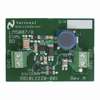
LM5008EVAL
Manufacturer Part Number
LM5008EVAL
Description
EVALUATION BOARD FOR LM5008
Manufacturer
National Semiconductor
Specifications of LM5008EVAL
Main Purpose
DC/DC, Step Down
Outputs And Type
1, Non-Isolated
Voltage - Output
10V
Current - Output
300mA
Voltage - Input
12 ~ 95V
Regulator Topology
Buck
Board Type
Fully Populated
Utilized Ic / Part
LM5008
Lead Free Status / RoHS Status
Contains lead / RoHS non-compliant
Power - Output
-
Frequency - Switching
-
Other names
*LM5008EVAL


On-Time Generator and Shutdown
The on-time for the LM5008 is determined by the R
and is inversely proportional to the input voltage (Vin), result-
ing in a nearly constant frequency as Vin is varied over its
range. The on-time equation for the LM5008 is:
See Figure 3. R
(at maximum V
Current Limit
The LM5008 contains an intelligent current limit OFF timer. If
the current in the Buck switch exceeds 0.5A the present cycle
is immediately terminated, and a non-resetable OFF timer is
initiated. The length of off-time is controlled by an external
resistor (R
0V, a maximum off-time is required, and the time is preset to
35µs. This condition occurs when the output is shorted, and
during the initial part of start-up. This amount of time ensures
safe short circuit operation up to the maximum input voltage
of 95V. In cases of overload where the FB voltage is above
zero volts (not a short circuit) the current limit off-time will be
less than 35µs. Reducing the off-time during less severe
overloads reduces the amount of foldback, recovery time, and
the start-up time. The off-time is calculated from the following
equation:
The current limit sensing circuit is blanked for the first 50-70ns
of each on-time so it is not falsely tripped by the current surge
which occurs at turn-on. The current surge is required by the
re-circulating diode (D1) for its turn-off recovery.
N - Channel Buck Switch and Driver
The LM5008 integrates an N-Channel Buck switch and as-
sociated floating high voltage gate driver. The gate driver
circuit works in conjunction with an external bootstrap capac-
itor and an internal high voltage diode. A 0.01µF ceramic
capacitor (C4) connected between the BST pin and SW pin
provides the voltage to the driver during the on-time.
During each off-time, the SW pin is at approximately 0V, and
the bootstrap capacitor charges from Vcc through the internal
diode. The minimum OFF timer, set to 300ns, ensures a min-
imum time each cycle to recharge the bootstrap capacitor.
An external re-circulating diode (D1) carries the inductor cur-
rent after the internal Buck switch turns off. This diode must
be of the Ultra-fast or Schottky type to minimize turn-on losses
and current over-shoot.
T
OFF
= 10
CL
T
) and the FB voltage (see Figure 5). When FB =
-5
ON
IN
ON
/ (0.285 + (V
) greater than 400 ns, for proper current limit
= 1.25 x 10
should be selected for a minimum on-time
-10
FB
/ 6.35 x 10
x R
ON
/ V
IN
-6
x R
FIGURE 11. Shutdown Implementation
CL
))
ON
resistor,
(2)
(3)
9
operation. This requirement limits the maximum frequency for
each application, depending on V
The LM5008 can be remotely disabled by taking the R
pin to ground. See Figure 11. The voltage at the R
is between 1.5 and 3.0 volts, depending on Vin and the value
of the R
Thermal Protection
The LM5008 should be operated so the junction temperature
does not exceed 125°C during normal operation. An internal
Thermal Shutdown circuit is provided to protect the LM5008
in the event of a higher than normal junction temperature.
When activated, typically at 165°C, the controller is forced into
a low power reset state, disabling the buck switch and the
V
accidental device overheating. When the junction tempera-
ture reduces below 140°C (typical hysteresis = 25°C), the Vcc
regulator is enabled, and normal operation is resumed.
Applications Information
SELECTION OF EXTERNAL COMPONENTS
A guide for determining the component values will be illus-
trated with a design example. Refer to Figure 1. The following
steps will configure the LM5008 for:
•
•
•
•
R1 and R2: From Figure 1, V
since V
Standard values of 3.01 kΩ (R1) and 1.00 kΩ (R2) are cho-
sen. Other values could be used as long as the 3:1 ratio is
maintained. The selected values, however, provide a small
amount of output loading (2.5 mA) in the event the main load
is disconnected. This allows the circuit to maintain regulation
until the main load is reconnected.
F
for the LM5008 is 50kHz to 600 kHz. Unless the application
requires a specific frequency, the choice of frequency is gen-
erally a compromise since it affects the size of L1 and C2, and
s
CC
and R
Input voltage range (Vin): 12V to 95V
Output voltage (V
Load current (for continuous conduction mode): 100 mA
to 300 mA
Maximum ripple at V
voltage
regulator. This feature prevents catastrophic failures from
FB
ON
ON
= 2.5V, the ratio of R1 to R2 calculates as 3:1.
resistor.
: The recommended operating frequency range
20097907
OUT1
OUT2
): 10V
: 100 mVp-p at maximum input
OUT1
IN
= V
and V
FB
x (R1 + R2) / R2, and
OUT
. See Figure 4.
www.national.com
ON
/SD pin
ON
/SD
Related parts for LM5008EVAL
Image
Part Number
Description
Manufacturer
Datasheet
Request
R

Part Number:
Description:
National Semiconductor [8-Bit D/A Converter]
Manufacturer:
National Semiconductor
Datasheet:
Part Number:
Description:
National Semiconductor [Media Coprocessor]
Manufacturer:
National Semiconductor
Datasheet:
Part Number:
Description:
Digitally Controlled Tone and Volume Circuit with Stereo Audio Power Amplifier, Microphone Preamp Stage and National 3D Sound
Manufacturer:
National Semiconductor
Datasheet:
Part Number:
Description:
Digitally Controlled Tone and Volume Circuit with Stereo Audio Power Amplifier, Microphone Preamp Stage and National 3D Sound
Manufacturer:
National Semiconductor
Datasheet:
Part Number:
Description:
AC97 Rev 2 Codec with Sample Rate Conversion and National 3D Sound
Manufacturer:
National Semiconductor
Part Number:
Description:
Manufacturer:
National Semiconductor
Datasheet:
Part Number:
Description:
Manufacturer:
National Semiconductor
Datasheet:
Part Number:
Description:
General Purpose, Low Voltage, Low Power, Rail-to-Rail Output Operational Amplifiers
Manufacturer:
National Semiconductor
Datasheet:
Part Number:
Description:
8-bit 20 MSPS flash A/D converter.
Manufacturer:
National Semiconductor
Datasheet:
Part Number:
Description:
Low Noise Quad Operational Amplifier
Manufacturer:
National Semiconductor
Datasheet:
Part Number:
Description:
Quad Differential Line Receivers
Manufacturer:
National Semiconductor
Datasheet:
Part Number:
Description:
Quad High Speed Trapezoidal? Bus Transceiver
Manufacturer:
National Semiconductor
Datasheet:
Part Number:
Description:
Dual Line Receiver
Manufacturer:
National Semiconductor
Datasheet:
Part Number:
Description:
TTL to 10k ECL Level Translator with Latch
Manufacturer:
National Semiconductor
Datasheet: