LM5008EVAL National Semiconductor, LM5008EVAL Datasheet - Page 10
LM5008EVAL
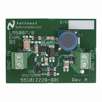
Manufacturer Part Number
LM5008EVAL
Description
EVALUATION BOARD FOR LM5008
Manufacturer
National Semiconductor
Specifications of LM5008EVAL
Main Purpose
DC/DC, Step Down
Outputs And Type
1, Non-Isolated
Voltage - Output
10V
Current - Output
300mA
Voltage - Input
12 ~ 95V
Regulator Topology
Buck
Board Type
Fully Populated
Utilized Ic / Part
LM5008
Lead Free Status / RoHS Status
Contains lead / RoHS non-compliant
Power - Output
-
Frequency - Switching
-
Other names
*LM5008EVAL


www.national.com
the switching losses. The maximum allowed frequency,
based on a minimum on-time of 400 ns, is calculated from:
For this exercise, Fmax = 263kHz. From equation 1, R
culates to 304 kΩ. A standard value 357 kΩ resistor will be
used to allow for tolerances in equation 1, resulting in a fre-
quency of 224kHz.
L1: The main parameter affected by the inductor is the output
current ripple amplitude. The choice of inductor value there-
fore depends on both the minimum and maximum load cur-
rents, keeping in mind that the maximum ripple current occurs
at maximum Vin.
a) Minimum load current: To maintain continuous conduc-
tion at minimum Io (100 mA), the ripple amplitude (I
be less than 200 mA p-p so the lower peak of the waveform
does not reach zero. L1 is calculated using the following
equation:
At Vin = 95V, L1(min) calculates to 200 µH. The next larger
standard value (220 µH) is chosen and with this value I
calculates to 181 mA p-p at Vin = 95V, and 34 mA p-p at Vin
= 12V.
b) Maximum load current: At a load current of 300 mA, the
peak of the ripple waveform must not reach the minimum
guaranteed value of the LM5008’s current limit threshold (410
mA). Therefore the ripple amplitude must be less than 220
mA p-p, which is already satisfied in the above calculation.
With L1 = 220 µH, at maximum Vin and Io, the peak of the
ripple will be 391 mA. While L1 must carry this peak current
without saturating or exceeding its temperature rating, it also
must be capable of carrying the maximum guaranteed value
of the LM5008’s current limit threshold (610 mA) without sat-
urating, since the current limit is reached during startup.
Starting when the current reaches Io (300 mA in Figure 12)
half way through the on-time, the current continues to in-
crease to the peak (391 mA), and then decreases to 300 mA
half way through the off-time. The average value of this por-
tion of the waveform is 45.5mA, and will cause half of the
voltage ripple, or 14 mV. The interval is one half of the fre-
quency cycle time, or 2.23 µs. Using the capacitor’s basic
equation:
the minimum value for C2 is 7.2 µF. The ripple due to C2’s
capacitance is 90° out of phase from the ESR ripple, and the
F
MAX
= V
C = I x Δt / ΔV
OUT
/ (V
INMAX
x 400ns)
FIGURE 12. Inductor Current Waveform
OR
ON
) must
cal-
OR
10
The DC resistance of the inductor should be as low as pos-
sible. For example, if the inductor’s DCR is one ohm, the
power dissipated at maximum load current is 0.09W. While
small, it is not insignificant compared to the load power of 3W.
C3: The capacitor on the V
filtering and stability, but its primary purpose is to prevent false
triggering of the V
tions. For this reason, C3 should be no smaller than 0.1 µF.
C2, and R3: When selecting the output filter capacitor C2, the
items to consider are ripple voltage due to its ESR, ripple
voltage due to its capacitance, and the nature of the load.
a) ESR and R3: A low ESR for C2 is generally desirable so
as to minimize power losses and heating within the capacitor.
However, a hysteretic regulator requires a minimum amount
of ripple voltage at the feedback input for proper loop opera-
tion. For the LM5008 the minimum ripple required at pin 5 is
25 mV p-p, requiring a minimum ripple at V
Since the minimum ripple current (at minimum Vin) is 34 mA
p-p, the minimum ESR required at V
2.94Ω. Since quality capacitors for SMPS applications have
an ESR considerably less than this, R3 is inserted as shown
in Figure 1. R3’s value, along with C2’s ESR, must result in
at least 25 mV p-p ripple at pin 5. Generally, R3 will be 0.5 to
3.0Ω.
b) Nature of the Load: The load can be connected to
V
ripple voltage which ranges from 100 mV (@ Vin = 12V) to
500mV (@Vin = 95V). Alternatively, V
ple, but lower regulation due to R3.
For a maximum allowed ripple voltage of 100 mVp-p at
V
maximum Vin, the ripple current is 181 mAp-p, creating a rip-
ple voltage of 72 mVp-p. This leaves 28 mVp-p of ripple due
to the capacitance. The average current into C2 due to the
ripple current is calculated using the waveform in Figure 12.
two numbers do not add directly. However, this calculation
provides a practical minimum value for C2 based on its ESR,
and the target spec. To allow for the capacitor’s tolerance,
temperature effects, and voltage effects, a 15 µF, X7R ca-
pacitor will be used.
c) In summary: The above calculations provide a minimum
value for C2, and a calculation for R3. The ESR is just as
important as the capacitance. The calculated values are
guidelines, and should be treated as starting points. For each
application, experimentation is needed to determine the op-
timum values for R3 and C2.
OUT1
OUT2
or V
(@ Vin = 95V), assume an ESR of 0.4Ω for C2. At
OUT2
. V
CC
OUT1
UVLO at the buck switch on/off transi-
provides good regulation, but with a
CC
output provides not only noise
OUT1
OUT2
is 100mV/34mA =
20097926
provides low rip-
OUT1
of 100 mV.
Related parts for LM5008EVAL
Image
Part Number
Description
Manufacturer
Datasheet
Request
R

Part Number:
Description:
National Semiconductor [8-Bit D/A Converter]
Manufacturer:
National Semiconductor
Datasheet:
Part Number:
Description:
National Semiconductor [Media Coprocessor]
Manufacturer:
National Semiconductor
Datasheet:
Part Number:
Description:
Digitally Controlled Tone and Volume Circuit with Stereo Audio Power Amplifier, Microphone Preamp Stage and National 3D Sound
Manufacturer:
National Semiconductor
Datasheet:
Part Number:
Description:
Digitally Controlled Tone and Volume Circuit with Stereo Audio Power Amplifier, Microphone Preamp Stage and National 3D Sound
Manufacturer:
National Semiconductor
Datasheet:
Part Number:
Description:
AC97 Rev 2 Codec with Sample Rate Conversion and National 3D Sound
Manufacturer:
National Semiconductor
Part Number:
Description:
Manufacturer:
National Semiconductor
Datasheet:
Part Number:
Description:
Manufacturer:
National Semiconductor
Datasheet:
Part Number:
Description:
General Purpose, Low Voltage, Low Power, Rail-to-Rail Output Operational Amplifiers
Manufacturer:
National Semiconductor
Datasheet:
Part Number:
Description:
8-bit 20 MSPS flash A/D converter.
Manufacturer:
National Semiconductor
Datasheet:
Part Number:
Description:
Low Noise Quad Operational Amplifier
Manufacturer:
National Semiconductor
Datasheet:
Part Number:
Description:
Quad Differential Line Receivers
Manufacturer:
National Semiconductor
Datasheet:
Part Number:
Description:
Quad High Speed Trapezoidal? Bus Transceiver
Manufacturer:
National Semiconductor
Datasheet:
Part Number:
Description:
Dual Line Receiver
Manufacturer:
National Semiconductor
Datasheet:
Part Number:
Description:
TTL to 10k ECL Level Translator with Latch
Manufacturer:
National Semiconductor
Datasheet: