551011367-011/NOPB National Semiconductor, 551011367-011/NOPB Datasheet - Page 13
551011367-011/NOPB
Manufacturer Part Number
551011367-011/NOPB
Description
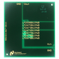
BOARD WEBENCH BUILD IT LM2598
Manufacturer
National Semiconductor
Series
WEBENCH® Buildit Boardr
Datasheet
1.LM2598T-12NOPB.pdf
(33 pages)
Specifications of 551011367-011/NOPB
Main Purpose
DC/DC, Step Down
Regulator Topology
Buck
Board Type
Bare (Unpopulated)
Utilized Ic / Part
LM2598, LM2670, LM2673, LM2676, LM2677, LM2678, LM2679
Lead Free Status / RoHS Status
Lead free / RoHS Compliant
Current - Output
-
Voltage - Output
-
Voltage - Input
-
Power - Output
-
Frequency - Switching
-
Outputs And Type
-
Other names
*551011367-011
*551011367-011/NOPB
551011367-011
*551011367-011/NOPB
551011367-011


LM2598 Series Buck Regulator Design Procedure (Adjustable Output)
PROCEDURE (Adjustable Output Voltage Version)
Given:
V
V
I
F = Switching Frequency (Fixed at a nominal 150 kHz).
1. Programming Output Voltage (Selecting R
shown in Figure 1 )
Use the following formula to select the appropriate resistor
values.
Select a value for R
resistor values minimize noise pickup in the sensitive feed-
back pin. (For the lowest temperature coefficient and the best
stability with time, use 1% metal film resistors.)
2. Inductor Selection (L1)
A. Calculate the inductor Volt • microsecond constant E • T
(V • µs), from the following formula:
where V
and V
B. Use the E • T value from the previous formula and match
it with the E • T number on the vertical axis of the Inductor
Value Selection Guide shown in Figure 7 .
C. on the horizontal axis, select the maximum load current.
D. Identify the inductance region intersected by the E • T
value and the Maximum Load Current value. Each region is
identified by an inductance value and an inductor code
(LXX).
E. Select an appropriate inductor from the four manufactur-
er’s part numbers listed in Figure 8 .
3. Output Capacitor Selection (C
A. In the majority of applications, low ESR electrolytic or solid
tantalum capacitors between 82 µF and 220 µF provide the
best results. This capacitor should be located close to the IC
using short capacitor leads and short copper traces. Do not
use capacitors larger than 220 µF. For additional informa-
tion, see section on output capacitors in application
information section.
LOAD
OUT
IN
(max) = Maximum Input Voltage
(max) = Maximum Load Current
D
= Regulated Output Voltage
= diode forward voltage drop = 0.5V
SAT
= internal switch saturation voltage = 1V
1
between 240
OUT
and 1.5 k . The lower
)
1
and R
2
, as
13
EXAMPLE (Adjustable Output Voltage Version)
Given:
V
I
F = Switching Frequency (Fixed at a nominal 150 kHz).
1. Programming Output Voltage (Selecting R
shown in Figure 1 )
Select R
R
R
2. Inductor Selection (L1)
A. Calculate the inductor Volt • microsecond constant
(E • T),
B. E • T = 34.8 (V • µs)
C. I
D. From the inductor value selection guide shown in Figure 7 ,
the inductance region intersected by the 35 (V • µs) horizon-
tal line and the 1A vertical line is 100 µH, and the inductor
code is L29.
E. From the table in Figure 8 , locate line L29, and select an
inductor part number from the list of manufacturers part
numbers.
3. Output Capacitor SeIection (C
A. See section on C
LOAD
IN
2
2
V
(max) = 28V
= 1k (16.26 − 1) = 15.26k, closest 1% value is 15.4 k .
= 15.4 k .
LOAD
OUT
(max) = 1A
= 20V
(max) = 1A
1
to be 1 k , 1%. Solve for R
OUT
in Application Information section.
OUT
2
)
.
1
www.national.com
and R
2
, as
Related parts for 551011367-011/NOPB
Image
Part Number
Description
Manufacturer
Datasheet
Request
R

Part Number:
Description:
WEBENCH Build It Unpopulated PCB For LM2598
Manufacturer:
National Semiconductor

Part Number:
Description:
BOARD WEBENCH LM2577,LM2585/87
Manufacturer:
National Semiconductor
Datasheet:

Part Number:
Description:
BOARD WEBENCH BUILD IT LM2586/88
Manufacturer:
National Semiconductor
Datasheet:

Part Number:
Description:
BOARD WEBENCH BUILD IT
Manufacturer:
National Semiconductor
Datasheet:

Part Number:
Description:
BOARD WEBENCH BUILD IT LM2599
Manufacturer:
National Semiconductor
Datasheet:

Part Number:
Description:
BOARD WEBENCH BUILD IT LM2595
Manufacturer:
National Semiconductor
Datasheet:

Part Number:
Description:
BOARD WEBENCH BUILD IT LM2586/88
Manufacturer:
National Semiconductor
Datasheet:
Part Number:
Description:
LM2577/86 BUILD IT BOARD
Manufacturer:
National Semiconductor
Part Number:
Description:
LM2585/8 BUILD IT BOARD
Manufacturer:
National Semiconductor
Part Number:
Description:
National Semiconductor [8-Bit D/A Converter]
Manufacturer:
National Semiconductor
Datasheet:
Part Number:
Description:
National Semiconductor [Media Coprocessor]
Manufacturer:
National Semiconductor
Datasheet:
Part Number:
Description:
Digitally Controlled Tone and Volume Circuit with Stereo Audio Power Amplifier, Microphone Preamp Stage and National 3D Sound
Manufacturer:
National Semiconductor
Datasheet:
Part Number:
Description:
Digitally Controlled Tone and Volume Circuit with Stereo Audio Power Amplifier, Microphone Preamp Stage and National 3D Sound
Manufacturer:
National Semiconductor
Datasheet:
Part Number:
Description:
AC97 Rev 2 Codec with Sample Rate Conversion and National 3D Sound
Manufacturer:
National Semiconductor
Part Number:
Description:
Manufacturer:
National Semiconductor
Datasheet: