STEVAL-ISA023V1 STMicroelectronics, STEVAL-ISA023V1 Datasheet - Page 26
STEVAL-ISA023V1
Manufacturer Part Number
STEVAL-ISA023V1
Description
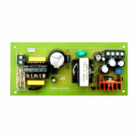
EVAL BOARD 24W POS OUT VIPER53E
Manufacturer
STMicroelectronics
Series
VIPER™r
Type
AC/DC Switching Convertersr
Specifications of STEVAL-ISA023V1
Mfg Application Notes
VIPer53EDIP - AppNote
Design Resources
STEVAL-ISA023V1 Gerber Files STEVAL-ISA023V1 Schematic STEVAL-ISA023V1 Bill of Materials
Main Purpose
AC/DC, Primary Side
Outputs And Type
3, Isolated
Power - Output
25W
Voltage - Output
5V, 12V, 3.3V
Current - Output
3A, 800mA, 100mA
Voltage - Input
90 ~ 265VAC
Regulator Topology
Flyback
Frequency - Switching
60kHz
Board Type
Fully Populated
Utilized Ic / Part
VIPer53
Input Voltage
90 V to 265 V
Output Voltage
3.3 V, 5 V, 12 V
Product
Power Management Modules
Silicon Manufacturer
ST Micro
Silicon Core Number
VIPer53-E
Kit Application Type
Power Management
Application Sub Type
SMPS
Kit Contents
Board
Rohs Compliant
Yes
Lead Free Status / RoHS Status
Lead free / RoHS Compliant
For Use With/related Products
VIPer53-E
Other names
497-5865


Transconductance error amplifier
26/36
optocoupler, the internal error amplifier is fully used for regulation). A typical schematic
corresponding to this situation can be seen on
The transfer function of the power cell is represented as G(s) in
which depends on the output load and on the output capacitor value. As the load of a
converter may change, two curves are shown for two different values of output resistance
value, R
capacitor ESR. Note: The overall transfer function does not depend on the input voltage
because of the current mode control.
The error amplifier has a fixed behavior, similar to the one shown in
is to avoid injection of high frequency noise in the current mode section. A zero due to the
R
The total transfer function is shown as F(s). G(s) at the bottom of
load (plain line), the load pole is exactly compensated by the zero of the error amplifier, and
the result is a perfect first order decreasing until it reaches the zero of the output capacitor
ESR. The error amplifier cut-off then definitely any further spurious noise or resonance from
disturbing the regulation loop.
The point where the complete transfer function has a unity gain is known as the regulation
bandwidth and has:
In
The dynamic load regulation is improved by increasing the regulation bandwidth, but some
limitations have to be respected: As the transfer function above the zero due the capacitor
ESR is not reliable (The ESR itself is not well specified, and other parasitic effects may take
place), the bandwidth should always be lower than the minimum of F
As the highest bandwidth is obtained with the highest output power (Plain line with R
in
value of R
range. The following formula can be derived:
Equation 12
With:
COMP
Figure
Figure
–
–
-C
P
L1
OUT2
COMP
24, the unity gain is reached in a first order slope, so the stability is ensured.
The higher it is, the faster the reaction will be to an eventual load change, and the
smaller the output voltage change will be.
The phase shift in the complete system at this point has to be less than 135° to
ensure good stability. Generally, a first-order slope gives 90° of phase shift, and a
second-order gives 180°.
24), the above criteria will be checked for this condition and allows to define the
COMP
and R
=
network is set at the same value as the maximum load R
, as the error amplifier gain depends only on this value for this frequency
V
--------------
L2
R
2
OUT
L2
. A zero at higher frequency values then appears, due to the output
R
COMP
=
P
---------------- -
P
OUT2
MAX
F
----------------------------------------------------- -
BW2
Figure
R
Gm
18.
L2
and:
C
OUT
P
MAX
Figure 24
=
Figure
Figure
C
1
-- -
2
and ESR zero.
L2
L
P
24. For maximum
Iexhibits a pole
23. Its bandwidth
pole.
I
2
LIM
VIPer53 - E
F
SW
L2
load
Related parts for STEVAL-ISA023V1
Image
Part Number
Description
Manufacturer
Datasheet
Request
R

Part Number:
Description:
BOARD RGB CTR ST7,STP08C596MTR
Manufacturer:
STMicroelectronics
Datasheet:

Part Number:
Description:
Power Management IC Development Tools Full Speed USB to RS232 Bridge Demo
Manufacturer:
STMicroelectronics
Datasheet:
Part Number:
Description:
Power Management IC Development Tools 2.5W solar eval BRD USB SPV1040 LD39050
Manufacturer:
STMicroelectronics
Datasheet:

Part Number:
Description:
BOARD EVAL FOR MEMS SENSORS
Manufacturer:
STMicroelectronics
Datasheet:

Part Number:
Description:
KIT DEV STARTER ST10F276Z5
Manufacturer:
STMicroelectronics
Datasheet:

Part Number:
Description:
BOARD EVAL HDMI $ VIDEO SWITCH
Manufacturer:
STMicroelectronics
Datasheet:

Part Number:
Description:
BOARD DEMO ACCELEROMETER DIL24
Manufacturer:
STMicroelectronics
Datasheet:

Part Number:
Description:
BOARD STLM75/STDS75/ST72F651
Manufacturer:
STMicroelectronics
Datasheet:

Part Number:
Description:
EVAL BOARD 3AXIS MEMS ACCELLRMTR
Manufacturer:
STMicroelectronics
Datasheet:

Part Number:
Description:
BOARD EVAL 8BIT MICRO + TDE1708
Manufacturer:
STMicroelectronics
Datasheet:
Part Number:
Description:
STMicroelectronics [RIPPLE-CARRY BINARY COUNTER/DIVIDERS]
Manufacturer:
STMicroelectronics
Datasheet:
Part Number:
Description:
STMicroelectronics [LIQUID-CRYSTAL DISPLAY DRIVERS]
Manufacturer:
STMicroelectronics
Datasheet:
Part Number:
Description:
BOARD EVAL FOR MEMS SENSORS
Manufacturer:
STMicroelectronics
Datasheet: