9397 750 16172 NXP Semiconductors, 9397 750 16172 Datasheet - Page 5
9397 750 16172
Manufacturer Part Number
9397 750 16172
Description
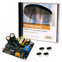
KIT DEMO STARPLUG BRONCO II
Manufacturer
NXP Semiconductors
Specifications of 9397 750 16172
Main Purpose
AC/DC, Primary Side
Outputs And Type
1, Isolated
Power - Output
6W
Voltage - Output
5V
Current - Output
1.2A
Voltage - Input
80 ~ 276VAC
Regulator Topology
Flyback
Board Type
Fully Populated
Utilized Ic / Part
TEA1522
Lead Free Status / RoHS Status
Lead free / RoHS Compliant
Frequency - Switching
-
Other names
568-4326


NXP Semiconductors
TEA152X
Product data sheet
8.1 Start-up and Underoltage lockout
8.2 Oscillator
8.3 Duty factor control
8.4 Valley switching
components R
Furthermore, a primary stroke is started only in a valley of the secondary ringing. This
valley switching principle minimizes capacitive switch-on losses.
Initially, the IC is self supplying from the rectified mains voltage. The IC starts switching as
soon as the voltage on pin V
the auxiliary winding of the transformer as soon as V
from the line is stopped for high efficiency operation.
When for some reason the auxiliary supply is not sufficient, the high-voltage supply also
supplies the IC. As soon as the voltage on pin V
stops switching and restarts from the rectified mains voltage.
The frequency of the oscillator is set by the external resistor and capacitor on pin RC. The
external capacitor is charged rapidly to the V
stroke, it discharges to the V
relative sensitivity of the duty factor to the regulation voltage at low duty factor is almost
equal to the sensitivity at high duty factors. This results in a more constant gain over the
duty factor range compared to PWM systems with a linear sawtooth oscillator. Stable
operation at low duty factors is easily realized. For high efficiency, the frequency is
reduced as soon as the duty factor drops below a certain value. This is accomplished by
increasing the oscillator charge time.
To ensure that the capacitor can be charged within the charge time, the value of the
oscillator capacitor should be limited to approximately 1 nF.
The duty factor is controlled by the internal regulation voltage and the oscillator signal on
pin RC. The internal regulation voltage is equal to the external regulation voltage (−2.5 V)
multiplied by the gain of the error amplifier (typically 20 dB which is 10×).
A new cycle is started when the primary switch is switched on (see
certain time (determined by the oscillator voltage RC and the internal regulation level), the
switch is turned off and the secondary stroke starts. The internal regulation level is
determined by the voltage on pin REG.
After the secondary stroke, the drain voltage shows an oscillation with a frequency of
approximately:
where:
--------------------------------------------- -
2
×
L
C
p
π
p
= primary self-inductance
= parasitic capacitance on drain node
×
1
(
L
p
×
C
RC
All information provided in this document is subject to legal disclaimers.
p
)
and C
Rev. 04 — 14 September 2010
RC
. This mode is called Pulse Width Modulation (PWM).
CC
RC(min)
passes the V
level. Because the discharge is exponential, the
RC(max)
CC(startup)
CC
drops below the V
level and, starting from a new primary
CC
SMPS ICs for low-power systems
level. The supply is taken over by
is high enough and the supply
Figure
CC(stop)
TEA152x
© NXP B.V. 2010. All rights reserved.
4). After a
level, the IC
5 of 20
(1)
Related parts for 9397 750 16172
Image
Part Number
Description
Manufacturer
Datasheet
Request
R

Part Number:
Description:
NXP Semiconductors designed the LPC2420/2460 microcontroller around a 16-bit/32-bitARM7TDMI-S CPU core with real-time debug interfaces that include both JTAG andembedded trace
Manufacturer:
NXP Semiconductors
Datasheet:

Part Number:
Description:
NXP Semiconductors designed the LPC2458 microcontroller around a 16-bit/32-bitARM7TDMI-S CPU core with real-time debug interfaces that include both JTAG andembedded trace
Manufacturer:
NXP Semiconductors
Datasheet:
Part Number:
Description:
NXP Semiconductors designed the LPC2468 microcontroller around a 16-bit/32-bitARM7TDMI-S CPU core with real-time debug interfaces that include both JTAG andembedded trace
Manufacturer:
NXP Semiconductors
Datasheet:
Part Number:
Description:
NXP Semiconductors designed the LPC2470 microcontroller, powered by theARM7TDMI-S core, to be a highly integrated microcontroller for a wide range ofapplications that require advanced communications and high quality graphic displays
Manufacturer:
NXP Semiconductors
Datasheet:
Part Number:
Description:
NXP Semiconductors designed the LPC2478 microcontroller, powered by theARM7TDMI-S core, to be a highly integrated microcontroller for a wide range ofapplications that require advanced communications and high quality graphic displays
Manufacturer:
NXP Semiconductors
Datasheet:
Part Number:
Description:
The Philips Semiconductors XA (eXtended Architecture) family of 16-bit single-chip microcontrollers is powerful enough to easily handle the requirements of high performance embedded applications, yet inexpensive enough to compete in the market for hi
Manufacturer:
NXP Semiconductors
Datasheet:
Part Number:
Description:
The XA-S3 device is a member of Philips Semiconductors? XA(eXtended Architecture) family of high performance 16-bitsingle-chip microcontrollers
Manufacturer:
NXP Semiconductors
Datasheet:

Part Number:
Description:
The NXP BlueStreak LH75401/LH75411 family consists of two low-cost 16/32-bit System-on-Chip (SoC) devices
Manufacturer:
NXP Semiconductors
Datasheet:
Part Number:
Description:
The NXP LPC3130/3131 combine an 180 MHz ARM926EJ-S CPU core, high-speed USB2
Manufacturer:
NXP Semiconductors
Datasheet:
Part Number:
Description:
The NXP LPC3141 combine a 270 MHz ARM926EJ-S CPU core, High-speed USB 2
Manufacturer:
NXP Semiconductors
Part Number:
Description:
The NXP LPC3143 combine a 270 MHz ARM926EJ-S CPU core, High-speed USB 2
Manufacturer:
NXP Semiconductors

Part Number:
Description:
The NXP LPC3152 combines an 180 MHz ARM926EJ-S CPU core, High-speed USB 2
Manufacturer:
NXP Semiconductors
Part Number:
Description:
The NXP LPC3154 combines an 180 MHz ARM926EJ-S CPU core, High-speed USB 2
Manufacturer:
NXP Semiconductors

Part Number:
Description:
Standard level N-channel enhancement mode Field-Effect Transistor (FET) in a plastic package using NXP High-Performance Automotive (HPA) TrenchMOS technology
Manufacturer:
NXP Semiconductors
Datasheet: