MCP1650DM-DDSC1 Microchip Technology, MCP1650DM-DDSC1 Datasheet - Page 5
MCP1650DM-DDSC1
Manufacturer Part Number
MCP1650DM-DDSC1
Description
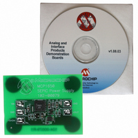
BOARD DEMO FOR MCP1650 SEPIC
Manufacturer
Microchip Technology
Type
DC/DC Switching Converters, Regulators & Controllersr
Specifications of MCP1650DM-DDSC1
Main Purpose
DC/DC, Step Up or Down
Outputs And Type
1, Non-Isolated
Voltage - Output
5V
Current - Output
160mA
Voltage - Input
3 ~ 7V
Regulator Topology
Boost
Frequency - Switching
750kHz
Board Type
Fully Populated
Utilized Ic / Part
MCP1650
Input Voltage
3 V to 7 V
Output Voltage
5 V
Product
Power Management Modules
For Use With/related Products
MCP1650R-E/MS
Lead Free Status / RoHS Status
Contains lead / RoHS non-compliant
Power - Output
-
Lead Free Status / Rohs Status
Lead free / RoHS Compliant


1.0
Absolute Maximum Ratings †
V
CS,FB,LBI,LBO,SHDN,PG,EXT............ GND – 0.3V to
Current at EXT pin ................................................ ±1A
Storage temperature .......................... -65°C to +150°C
Operating Junction Temperature........ -40°C to +125°C
ESD protection on all pins
DC CHARACTERISTICS
Electrical Specifications: Unless otherwise noted, all parameters apply at V
T
Input Characteristics
Supply Voltage
Undervoltage Lockout
(S Option)
Under Voltage Lockout
(R Option)
Undervoltage Hysteresis
Shutdown Supply Current
Quiescent Supply Current
Soft Start Time
Feedback Characteristics
Feedback Voltage
Feedback Comparator
Hysteresis
Feedback Input Bias Current
Current Sense Input
Current Sense Threshold
Delay from Current Sense to
Output
Ext Drive
EXT Driver ON Resistance
(High Side)
EXT Driver ON Resistance
(Low Side)
Oscillator Characteristics
Switching Frequency
Low Duty Cycle Switch-Over
Voltage
Duty Cycle Switch Voltage
Hysteresis
Low Duty Cycle
High Duty Cycle
IN TO
J
2004 Microchip Technology Inc.
= -40°C to +125°C. Typical values apply for V
GND........................................................... 6.0V
ELECTRICAL
CHARACTERISTICS
Parameters
UVLO
T
V
DC
I
DC
DC
UVLO
UVLO
SNS-TH
dly_ISNS
R
R
LowDuty
V
F
Sym
I
I
T
V
V
SHD
FBlk
HIGH
LOW
OSC
HYS
I
HIGH
SS
Q
FB
LOW
IN
Hyst
HYST
V
IN
4 kV HBM
+ 0.3V
1.85
1.18
Min
650
IN
2.7
2.4
-50
75
50
72
—
—
—
—
—
—
—
—
—
—
= 3.3V, T
0.001
2.55
1.22
Typ
117
120
500
114
750
2.0
3.8
—
12
—
80
92
56
80
8
4
A
+25°C.
† Notice: Stresses above those listed under “Maximum Rat-
ings” may cause permanent damage to the device. This is a
stress rating only and functional operation of the device at
those or any other conditions above those indicated in the
operational listings of this specification is not implied. Expo-
sure to maximum rating conditions for extended periods may
affect device reliability.
Max
2.15
1.26
220
155
850
5.5
2.7
23
50
18
12
62
88
—
—
—
—
—
1
MCP1650/51/52/53
Units
kHz
mV
mV
mV
mV
µA
µA
nA
µs
ns
%
%
V
V
V
V
V
IN
= +2.7V to +5.5V, SHDN = High,
V
V
SHDN = GND
EXT = Open
All conditions
V
V
IN
IN
FB
IN
rising edge
rising edge
rising edge
< 1.3V
Conditions
DS21876A-page 5
Related parts for MCP1650DM-DDSC1
Image
Part Number
Description
Manufacturer
Datasheet
Request
R

Part Number:
Description:
BOARD DEMO FOR MCP1650 WHITE LED
Manufacturer:
Microchip Technology
Datasheet:

Part Number:
Description:
BOARD DEMO FOR MCP165X
Manufacturer:
Microchip Technology
Datasheet:

Part Number:
Description:
Manufacturer:
Microchip Technology Inc.
Datasheet:
Part Number:
Description:
Manufacturer:
Microchip Technology Inc.
Datasheet:
Part Number:
Description:
Manufacturer:
Microchip Technology Inc.
Datasheet:
Part Number:
Description:
Manufacturer:
Microchip Technology Inc.
Datasheet:
Part Number:
Description:
Manufacturer:
Microchip Technology Inc.
Datasheet:
Part Number:
Description:
Manufacturer:
Microchip Technology Inc.
Datasheet:
Part Number:
Description:
Manufacturer:
Microchip Technology Inc.
Datasheet:
Part Number:
Description:
Manufacturer:
Microchip Technology Inc.
Datasheet: