MCP1650DM-DDSC1 Microchip Technology, MCP1650DM-DDSC1 Datasheet - Page 15
MCP1650DM-DDSC1
Manufacturer Part Number
MCP1650DM-DDSC1
Description
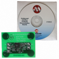
BOARD DEMO FOR MCP1650 SEPIC
Manufacturer
Microchip Technology
Type
DC/DC Switching Converters, Regulators & Controllersr
Specifications of MCP1650DM-DDSC1
Main Purpose
DC/DC, Step Up or Down
Outputs And Type
1, Non-Isolated
Voltage - Output
5V
Current - Output
160mA
Voltage - Input
3 ~ 7V
Regulator Topology
Boost
Frequency - Switching
750kHz
Board Type
Fully Populated
Utilized Ic / Part
MCP1650
Input Voltage
3 V to 7 V
Output Voltage
5 V
Product
Power Management Modules
For Use With/related Products
MCP1650R-E/MS
Lead Free Status / RoHS Status
Contains lead / RoHS non-compliant
Power - Output
-
Lead Free Status / Rohs Status
Lead free / RoHS Compliant


5.0
5.1
The MCP1650/51/52/53 boost controller can be used in
several different configurations and in many different
applications. For applications that require minimum
space, low cost and high efficiency, the MCP1650/51/
52/53 product family is a good choice. It can be used in
boost, buck-boost, Single-Ended Primary Inductive
Converters (SEPIC), as well as in flyback converter
topologies.
FIGURE 5-1:
2004 Microchip Technology Inc.
Input
Voltage
3.3V ±10%
APPLICATION CIRCUITS/
ISSUES
Typical Applications
C
IN
Typical Non-Bootstrap Application Circuit (MCP1650/51/52/53).
10 µF
off
on
SHDN
GND
V
NC
IN
3.3V to 12V 100 mA Boost Converter
8
2
6
5
MCP1650
R
0.05
SENSE
4
3
1
7
CS
EXT
NC
FB
5.1.1
Non-bootstrap applications are typically used when the
output voltage is boosted to a voltage that is higher
than the rated voltage of the MCP1650/51/52/53. For
non-bootstrap applications, the input voltage is
connected to the boost inductor through the optional
current sense resistor and the V
51/52/53. For this type of application, the S-option
devices (UVLO at 2.55V, typical) should be used. The
gated oscillator duty cycle will be dependant on the
value of the voltage on V
will be 56%. If V
In non-bootstrap applications, output voltages of over
100V can be generated. Even though the MCP1650/
51/52/53 device is not connected to the high boost
output voltage, the drain of the external MOSFET and
reverse voltage of the external Schottky diode are
connected. The output voltage capacitor must also be
rated for the output voltage.
Inductor
3.3 µH
Boost
MCP1650/51/52/53
Combination Device
MOSFET/Schottky
NON-BOOTSTRAP BOOST
APPLICATIONS
IN
< 3.8V, the duty cycle will be 80%.
IN
90.9 k
10 k
. If V
IN
IN
> 3.8V, the duty cycle
pin of the MCP1650/
C
10 µF
Ceramic
OUT
V
I
DS21876A-page 15
OUT
OUT
= 0 to 100 mA
= 12V
Related parts for MCP1650DM-DDSC1
Image
Part Number
Description
Manufacturer
Datasheet
Request
R

Part Number:
Description:
BOARD DEMO FOR MCP1650 WHITE LED
Manufacturer:
Microchip Technology
Datasheet:

Part Number:
Description:
BOARD DEMO FOR MCP165X
Manufacturer:
Microchip Technology
Datasheet:

Part Number:
Description:
Manufacturer:
Microchip Technology Inc.
Datasheet:
Part Number:
Description:
Manufacturer:
Microchip Technology Inc.
Datasheet:
Part Number:
Description:
Manufacturer:
Microchip Technology Inc.
Datasheet:
Part Number:
Description:
Manufacturer:
Microchip Technology Inc.
Datasheet:
Part Number:
Description:
Manufacturer:
Microchip Technology Inc.
Datasheet:
Part Number:
Description:
Manufacturer:
Microchip Technology Inc.
Datasheet:
Part Number:
Description:
Manufacturer:
Microchip Technology Inc.
Datasheet:
Part Number:
Description:
Manufacturer:
Microchip Technology Inc.
Datasheet: