NCP1605FORWGEVB ON Semiconductor, NCP1605FORWGEVB Datasheet - Page 4
NCP1605FORWGEVB
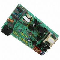
Manufacturer Part Number
NCP1605FORWGEVB
Description
EVAL BOARD FOR NCP1605FORWG
Manufacturer
ON Semiconductor
Datasheets
1.NCP1217P100G.pdf
(19 pages)
2.NCP1605ADR2G.pdf
(32 pages)
3.NCP1605FORWGEVB.pdf
(2 pages)
4.NCP1605FORWGEVB.pdf
(20 pages)
Specifications of NCP1605FORWGEVB
Design Resources
NCP1605FORWGEVB BOM NCP1605FORWGEVB Gerber Files NCP1605 EVB Schematic
Main Purpose
AC/DC, Primary and Secondary Side with PFC
Outputs And Type
1, Isolated
Voltage - Output
19V
Current - Output
8A
Voltage - Input
90 ~ 265VAC
Regulator Topology
Forward Converter
Frequency - Switching
133kHz
Board Type
Fully Populated
Utilized Ic / Part
NCP1217, NCP1605
Lead Free Status / RoHS Status
Lead free / RoHS Compliant
Power - Output
-
Lead Free Status / Rohs Status
Lead free / RoHS Compliant
For Use With/related Products
NCP1605FORWG
Other names
NCP1605FORWGEVBOS


1. Maximum Value @ T
2. Minimum Value @ T
ELECTRICAL CHARACTERISTICS
V
SUPPLY SECTION (All frequency versions, unless otherwise noted)
INTERNAL STARTUP CURRENT SOURCE (T
DRIVE OUTPUT
CURRENT COMPARATOR (Pin 5 Unloaded)
INTERNAL OSCILLATOR (V
Turn--On Threshold Level, V
Minimum Operating Voltage After Turn--On
V
Internal IC Consumption, No Output Load on Pin 5,
F
Internal IC Consumption, No Output Load on Pin 5,
F
Internal IC Consumption, No Output Load on Pin 5,
F
Internal IC Consumption, 1.0 nF Output Load on Pin 5,
F
Internal IC Consumption, 1.0 nF Output Load on Pin 5,
F
Internal IC Consumption, 1.0 nF Output Load on Pin 5,
F
Internal IC Consumption, Latchoff Phase, V
High--Voltage Current Source, V
High--Voltage Current Source, V
Output Voltage Rise--Time @ CL = 1.0 nF, 10--90% of a 12 V
Output Signal
Output Voltage Fall--Time @ CL = 1.0 nF, 10--90% of a 12 V
Output Signal
Source Resistance
Sink Resistance
Input Bias Current @ 1.0 V Input Level on Pin 3
Maximum Internal Current Setpoint
Default Internal Current Setpoint for Skip Cycle Operation
Propagation Delay from Current Detection to Gate OFF State
Leading Edge Blanking Duration
Oscillation Frequency, 65 kHz Version
Oscillation Frequency, 100 kHz Version
Oscillation Frequency, 133 kHz Version
Maximum Duty--Cycle, NCP1217
Maximum Duty--Cycle, NCP1217A
CC
SW
SW
SW
SW
SW
SW
CC
= 11 V unless otherwise noted.)
Decreasing Level at which the Latchoff Phase Ends
= 65 kHz
= 100 kHz
= 133 kHz
= 65 kHz
= 100 kHz
= 133 kHz
J
J
= 125C.
= 0C.
Characteristic
CC
CC
Going Up
= 11 V, Pin 5 Loaded by 1.0 kΩ)
CC
CC
= 10 V
= 0
(For typical values T
CC
J
= 6.0 V
> 0C)
http://onsemi.com
J
= 25C, for min/max values T
4
Pin
6
6
6
6
6
6
6
6
6
6
8
8
5
5
5
5
3
3
3
3
3
--
--
--
--
--
VCC
Symbol
VCC
VCC
Dmax
Dmax
ICC1
ICC1
ICC1
ICC2
ICC2
ICC2
ICC3
I
T
T
f
f
f
R
I
R
Lskip
IC1
IC2
Limit
OSC
OSC
OSC
I
T
T
DEL
LEB
OH
IB
OL
r
latch
f
min
ON
J
= 0C to +125C, Max T
(Note 2)
11.8
58.5
Min
120
6.9
3.5
5.0
0.9
15
90
69
42
--
--
--
--
--
--
--
--
--
--
--
--
--
--
--
1020
1060
12.8
0.02
46.5
Typ
960
230
330
250
100
133
7.6
5.6
1.7
2.1
2.4
6.0
7.0
1.0
60
20
20
10
90
65
74
J
(Note 1)
(Note 1)
(Note 1)
(Note 1)
(Note 1)
(Note 1)
= 150C,
1180
1200
1110
Max
13.8
71.5
150
110
146
8.3
2.0
2.4
2.9
7.8
1.1
35
18
80
50
--
--
--
--
--
--
--
--
Unit
kHz
kHz
kHz
mA
mA
mA
mA
mA
mV
mA
mA
mA
mA
mA
ns
ns
ns
ns
%
%
Ω
Ω
V
V
V
V
Related parts for NCP1605FORWGEVB
Image
Part Number
Description
Manufacturer
Datasheet
Request
R

Part Number:
Description:
ON Semiconductor [VOLTAGE REGULATOR]
Manufacturer:
ON Semiconductor
Datasheet:
Part Number:
Description:
357-036-542-201 CARDEDGE 36POS DL .156 BLK LOPRO
Manufacturer:
ON Semiconductor
Datasheet:
Part Number:
Description:
357-036-542-201 CARDEDGE 36POS DL .156 BLK LOPRO
Manufacturer:
ON Semiconductor
Datasheet:
Part Number:
Description:
357-036-542-201 CARDEDGE 36POS DL .156 BLK LOPRO
Manufacturer:
ON Semiconductor
Datasheet:
Part Number:
Description:
357-036-542-201 CARDEDGE 36POS DL .156 BLK LOPRO
Manufacturer:
ON Semiconductor
Datasheet:
Part Number:
Description:
357-036-542-201 CARDEDGE 36POS DL .156 BLK LOPRO
Manufacturer:
ON Semiconductor
Datasheet:
Part Number:
Description:
357-036-542-201 CARDEDGE 36POS DL .156 BLK LOPRO
Manufacturer:
ON Semiconductor
Datasheet:
Part Number:
Description:
357-036-542-201 CARDEDGE 36POS DL .156 BLK LOPRO
Manufacturer:
ON Semiconductor
Datasheet:
Part Number:
Description:
357-036-542-201 CARDEDGE 36POS DL .156 BLK LOPRO
Manufacturer:
ON Semiconductor
Datasheet:
Part Number:
Description:
357-036-542-201 CARDEDGE 36POS DL .156 BLK LOPRO
Manufacturer:
ON Semiconductor
Datasheet:
Part Number:
Description:
357-036-542-201 CARDEDGE 36POS DL .156 BLK LOPRO
Manufacturer:
ON Semiconductor
Datasheet:
Part Number:
Description:
Manufacturer:
ON Semiconductor
Datasheet:
Part Number:
Description:
Manufacturer:
ON Semiconductor
Datasheet:
Part Number:
Description:
Manufacturer:
ON Semiconductor
Datasheet: