NCP1605FORWGEVB ON Semiconductor, NCP1605FORWGEVB Datasheet - Page 13
NCP1605FORWGEVB
Manufacturer Part Number
NCP1605FORWGEVB
Description
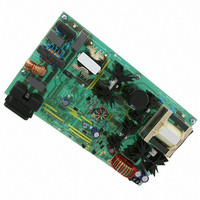
EVAL BOARD FOR NCP1605FORWG
Manufacturer
ON Semiconductor
Datasheets
1.NCP1217P100G.pdf
(19 pages)
2.NCP1605ADR2G.pdf
(32 pages)
3.NCP1605FORWGEVB.pdf
(2 pages)
4.NCP1605FORWGEVB.pdf
(20 pages)
Specifications of NCP1605FORWGEVB
Design Resources
NCP1605FORWGEVB BOM NCP1605FORWGEVB Gerber Files NCP1605 EVB Schematic
Main Purpose
AC/DC, Primary and Secondary Side with PFC
Outputs And Type
1, Isolated
Voltage - Output
19V
Current - Output
8A
Voltage - Input
90 ~ 265VAC
Regulator Topology
Forward Converter
Frequency - Switching
133kHz
Board Type
Fully Populated
Utilized Ic / Part
NCP1217, NCP1605
Lead Free Status / RoHS Status
Lead free / RoHS Compliant
Power - Output
-
Lead Free Status / Rohs Status
Lead free / RoHS Compliant
For Use With/related Products
NCP1605FORWG
Other names
NCP1605FORWGEVBOS


level, the default one or lower. As soon as some external
signal pulls this Adj pin level above 3.1 V typical, the output
pulses are permanently disabled. Care must be taken to limit
the injected current into pin 1 to less than 2.0 mA, e.g.
through a series resistor of 5.6 k with a 10 V V
startup switch is activated every time V
maintains a V
5.6 V and 12.8 V. Reset occurs when V
e.g. when the user cycle the SMPS down. Figure 25
illustrates the operation. Adding a zener diode from Q1 base
to ground makes a cheap OVP, protecting the supply from
any lethal open- -loop operation. If a thermistor (NTC) is
added in parallel with the Zener- -diode, overtemperature
protection is also ensured.
In normal operation, the Adj pin level is kept at a fixed
Figure 24. When Vadj is Pulled Above 3.1 V, NCP1217 Permanently Latches- -Off the Output Pulses
CC
voltage ramping up and down between
VCC
VCC
VCC
ON
latch
min
= 12.8 V
= 7.6 V
= 5.6 V
V
Drv
Adj
CC
CC
CC
reaches 5.6 V and
falls below 5.6 V,
adj level
Fault brings adj above latching level
Default
Driver
Pulses
CC
http://onsemi.com
. The
Reset level
13
The startup current source keeps the
device latched until reset occurs.
Latched--off
Nonlatching Shutdown
temporarily and authorize its restart once the default has
disappeared. This option can easily be accomplished
through a single NPN bipolar transistor wired between FB
and ground. By pulling FB below the Adj Pin 1 level, the
output pulses are disabled as long as FB is pulled below
Pin 1. As soon as FB is relaxed, the IC resumes its operation.
Figure 26 depicts the application example.
T
In some cases, it might be desirable to shut off the part
Figure 25. A Thermistor and a Zener Diode Offer
Both OVP and Overtemperature Latched- -Off
OVP
Protection
1
2
3
4
Vaux
Time
Time
Time
8
7
6
5
<16 V
CV
CC
Laux
Related parts for NCP1605FORWGEVB
Image
Part Number
Description
Manufacturer
Datasheet
Request
R

Part Number:
Description:
ON Semiconductor [VOLTAGE REGULATOR]
Manufacturer:
ON Semiconductor
Datasheet:
Part Number:
Description:
357-036-542-201 CARDEDGE 36POS DL .156 BLK LOPRO
Manufacturer:
ON Semiconductor
Datasheet:
Part Number:
Description:
357-036-542-201 CARDEDGE 36POS DL .156 BLK LOPRO
Manufacturer:
ON Semiconductor
Datasheet:
Part Number:
Description:
357-036-542-201 CARDEDGE 36POS DL .156 BLK LOPRO
Manufacturer:
ON Semiconductor
Datasheet:
Part Number:
Description:
357-036-542-201 CARDEDGE 36POS DL .156 BLK LOPRO
Manufacturer:
ON Semiconductor
Datasheet:
Part Number:
Description:
357-036-542-201 CARDEDGE 36POS DL .156 BLK LOPRO
Manufacturer:
ON Semiconductor
Datasheet:
Part Number:
Description:
357-036-542-201 CARDEDGE 36POS DL .156 BLK LOPRO
Manufacturer:
ON Semiconductor
Datasheet:
Part Number:
Description:
357-036-542-201 CARDEDGE 36POS DL .156 BLK LOPRO
Manufacturer:
ON Semiconductor
Datasheet:
Part Number:
Description:
357-036-542-201 CARDEDGE 36POS DL .156 BLK LOPRO
Manufacturer:
ON Semiconductor
Datasheet:
Part Number:
Description:
357-036-542-201 CARDEDGE 36POS DL .156 BLK LOPRO
Manufacturer:
ON Semiconductor
Datasheet:
Part Number:
Description:
357-036-542-201 CARDEDGE 36POS DL .156 BLK LOPRO
Manufacturer:
ON Semiconductor
Datasheet:
Part Number:
Description:
Manufacturer:
ON Semiconductor
Datasheet:
Part Number:
Description:
Manufacturer:
ON Semiconductor
Datasheet:
Part Number:
Description:
Manufacturer:
ON Semiconductor
Datasheet: