NCP1606BOOSTGEVB ON Semiconductor, NCP1606BOOSTGEVB Datasheet - Page 5
NCP1606BOOSTGEVB
Manufacturer Part Number
NCP1606BOOSTGEVB
Description
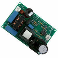
EVAL BOARD FOR NCP1606BOOSTG
Manufacturer
ON Semiconductor
Specifications of NCP1606BOOSTGEVB
Design Resources
NCP1606BOOST EVB BOM NCP1606BOOSTGEVB Gerber Files NCP1606BOOST EVB Schematic
Main Purpose
AC/DC, Primary and Secondary Side with PFC
Outputs And Type
1, Isolated
Power - Output
100W
Voltage - Output
400V
Current - Output
250mA
Voltage - Input
88 ~ 264VAC
Regulator Topology
Boost
Frequency - Switching
250kHz
Board Type
Fully Populated
Utilized Ic / Part
NCP1606
Lead Free Status / RoHS Status
Lead free / RoHS Compliant
For Use With/related Products
NCP1606BOOSTG
Other names
NCP1606BOOSTGEVBOS


RAMP CONTROL
OVER AND UNDERVOLTAGE PROTECTION
GATE DRIVE SECTION
3. Parameter values are valid for transient conditions only.
4. Parameter characterized and guaranteed by design, but not tested in production.
ELECTRICAL C
(Unless otherwise specified: For typical values, T
1 nF, Ct = 1 nF, CS = 0 V, Control = open, ZCD = open)
t
CT(discharge)
V
I
V
V
I
OVP(HYS)
Symbol
I
V
CL(NEG)
CHARGE
OUT(start)
t
CL(NEG)
V
SD
t
V
V
V
START
t
CTMAX
t
SYNC
I
R
R
PWM
t
OVP
ZCD
t
SD
SD
OVP
UVP
rise
fall
OH
HYS
OL
H
L
Negative Active Clamp Voltage @ I
Current Capability of the Negative Active Clamp:
in normal mode (V
in shutdown mode (V
Shutdown Threshold (V
Enable Threshold (V
Shutdown Comparator Hysteresis
Zero current detection propagation delay
Minimum detectable ZCD pulse width
Drive off restart timer
Charge Current (V
Time to discharge a 1 nF Ct capacitor from V
Maximum Ct level before DRV switches off
Propagation delay of the PWM comparator
Dynamic overvoltage protection (OVP) triggering current:
NCP1606A
NCP1606B @ T
NCP1606B @ T
Hysteresis of the dynamic OVP current before the OVP latch is released:
NCP1606A
NCP1606B
Static OVP Threshold Voltage
Undervoltage protection (UVP) threshold voltage
Gate Drive Resistance:
Drive voltage rise time from 10% V
Drive voltage fall time from 90% V
Driver output voltage at V
HARACTERISTICS
R
R
R
R
OH
OH
OL
OL
@ I
@ I
@ I
@ I
J
J
= 25°C
= −40°C to +125°C
ZCD
CT
SINK
SINK
SOURCE
SOURCE
ZCD
ZCD
= 0 V)
= 300 mV)
ZCD
= 100 mA
= 20 mA
rising)
= 100 mV)
CC
= 100 mA
= 20 mA
falling)
= V
CC(on)
J
CC
CC
= 25°C. For min/max values, T
ZCD
to 90% V
to 10% V
Rating
− 200 mV and I
= −2.5 mA
http://onsemi.com
CT
CC
CC
= 3.4 V to 100 mV.
with C
with C
5
sink
DRV
DRV
= 10 mA
= 1 nF and V
= 1 nF and V
−25°C < T
−40°C < T
−25°C < T
−40°C < T
J
= −40°C to +125°C, V
CC
J
J
J
J
CC
< +125°C
< +125°C
< +125°C
< +125°C
= 12 V.
= 12 V.
0.45
0.25
Min
150
243
235
2.5
2.9
2.9
9.0
8.7
CC
35
75
34
−
−
−
−
−
−
−
−
−
−
−
−
−
−
−
= 12 V, FB = 2.4 V, C
100 mV
V
10.4
EAL
Typ
200
290
100
180
270
270
150
0.6
3.7
3.2
3.2
8.5
0.3
70
90
70
40
30
12
12
30
25
−
−
6
6
−
+
Max
0.75
12.1
11.8
100
250
350
170
300
297
297
100
220
5.0
3.3
3.4
0.4
0.2
45
18
18
10
10
80
70
−
−
−
−
DRV
=
Unit
mA
mV
mV
mV
mA
mA
mA
mA
ns
ns
ms
ns
ns
ns
ns
V
V
V
V
W
V
Related parts for NCP1606BOOSTGEVB
Image
Part Number
Description
Manufacturer
Datasheet
Request
R

Part Number:
Description:
Cost Effective Power Factor Controller
Manufacturer:
ON Semiconductor
Datasheet:
Part Number:
Description:
ON Semiconductor [VOLTAGE REGULATOR]
Manufacturer:
ON Semiconductor
Datasheet:
Part Number:
Description:
357-036-542-201 CARDEDGE 36POS DL .156 BLK LOPRO
Manufacturer:
ON Semiconductor
Datasheet:
Part Number:
Description:
357-036-542-201 CARDEDGE 36POS DL .156 BLK LOPRO
Manufacturer:
ON Semiconductor
Datasheet:
Part Number:
Description:
357-036-542-201 CARDEDGE 36POS DL .156 BLK LOPRO
Manufacturer:
ON Semiconductor
Datasheet:
Part Number:
Description:
357-036-542-201 CARDEDGE 36POS DL .156 BLK LOPRO
Manufacturer:
ON Semiconductor
Datasheet:
Part Number:
Description:
357-036-542-201 CARDEDGE 36POS DL .156 BLK LOPRO
Manufacturer:
ON Semiconductor
Datasheet:
Part Number:
Description:
357-036-542-201 CARDEDGE 36POS DL .156 BLK LOPRO
Manufacturer:
ON Semiconductor
Datasheet:
Part Number:
Description:
357-036-542-201 CARDEDGE 36POS DL .156 BLK LOPRO
Manufacturer:
ON Semiconductor
Datasheet:
Part Number:
Description:
357-036-542-201 CARDEDGE 36POS DL .156 BLK LOPRO
Manufacturer:
ON Semiconductor
Datasheet:
Part Number:
Description:
357-036-542-201 CARDEDGE 36POS DL .156 BLK LOPRO
Manufacturer:
ON Semiconductor
Datasheet:
Part Number:
Description:
357-036-542-201 CARDEDGE 36POS DL .156 BLK LOPRO
Manufacturer:
ON Semiconductor
Datasheet:
Part Number:
Description:
Manufacturer:
ON Semiconductor
Datasheet:
Part Number:
Description:
Manufacturer:
ON Semiconductor
Datasheet: