NCP3163BSTEVB ON Semiconductor, NCP3163BSTEVB Datasheet - Page 4
NCP3163BSTEVB
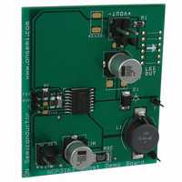
Manufacturer Part Number
NCP3163BSTEVB
Description
EVAL BOARD FOR NCP3163BST
Manufacturer
ON Semiconductor
Specifications of NCP3163BSTEVB
Design Resources
NCP3163 Boost Eval Board BOM NCP3163BSTEVB Gerber Files NCP3163 Boost Eval Board Schematic
Main Purpose
DC/DC, Step Up
Outputs And Type
1, Non-Isolated
Voltage - Output
24V
Current - Output
700mA
Voltage - Input
12V
Regulator Topology
Boost
Frequency - Switching
300kHz
Board Type
Fully Populated
Utilized Ic / Part
NCP3163
Lead Free Status / RoHS Status
Lead free / RoHS Compliant
Power - Output
-
Lead Free Status / Rohs Status
Lead free / RoHS Compliant
For Use With/related Products
NCP3163BST
Other names
NCP3163BSTEVBOS


5. Maximum package power dissipation limits must be observed.
6. Low duty cycle pulse techniques are used during test to maintain junction temperature as close to ambient as possible.
7. T
ELECTRICAL CHARACTERISTICS
values T
OSCILLATOR
FEEDBACK COMPARATOR 1
FEEDBACK COMPARATOR 2
CURRENT LIMIT COMPARATOR
DRIVER AND OUTPUT SWITCH (Note 6)
LOW VOLTAGE INDICATOR
TOTAL DEVICE
Frequency
Charge Current
Discharge Current
Charge to Discharge Current Ratio
Sawtooth Peak Voltage
Sawtooth Valley Voltage
Threshold Voltage
Threshold Voltage − Line Regulation (V
Input Bias Current (V
Threshold Voltage
Threshold Voltage − Line Regulation (V
Input Bias Current (V
Threshold Voltage
Input Bias Current (V
Saturation Voltage (I
Collector Off−State Leakage Current (V
Bootstrap Input Current Source (V
Bootstrap Input Zener Clamp Voltage (I
Input Threshold (V
Input Hysteresis (V
Output Sink Saturation Voltage (I
Output Off−State Leakage Current (V
Standby Supply Current (V
Non−Darlington (R
Darlington Connection (Pins 9, 10, 11 connected)
T
Total Variation over V
T
Total Variation over V
T
Total Variation over V
T
Total Variation over V
Pins 6, 14, 15 = GND, remaining pins open)
low
A
A
A
A
= 25°C, V
= 25°C
= 25°C, V
= 25°C
= 0°C for NCP3163
= − 40°C for NCP3163B
= − 40°C for NCV3163
A
is the operating ambient temperature range that applies (Note 7), unless otherwise noted.)
CC
CC
= 15 V
= 15 V
FB2
FB2
Pin 9
SW
FB1
FB2
Ipk (Sense)
Increasing)
Decreasing)
CC
CC
CC
CC
= 2.5 A, Pins 14, 15 grounded)
= 110 W to V
= 5.05 V)
= 1.25 V)
CC
Characteristic
= 2.5 V to 40 V and Temperature
= 2.5 V to 40 V and Temperature
= 2.5 V to 40 V and Temperature
= 2.5 V to 40 V, and Temperature
= 2.5 V to 40 V, Pin 8 = V
= 15 V)
sink
BS
= 2.0 mA)
CC
= V
OH
T
Z
CE
CC
CC
, I
high
= 15 V)
CC
(V
= 25 mA)
SW
= 40 V)
= 2.5 V to 40 V, T
= 2.5 V to 40 V, T
CC
+ 5.0 V)
= + 70°C for NCP3163
= + 85°C for NCP3163B
= + 125°C for NCV3163
/I
DRV
= 15 V, Pin 16 = V
≈ 20)
CC
http://onsemi.com
,
NCP3163
NCV3163
A
A
NCP3163
NCV3163
NCP3163
NCV3163
= 25°C)
= 25°C)
CC
4
, C
T
= 270 pF, R
REGline
REGline
I
I
source(DRV)
V
chg
I
Symbol
V
V
V
V
IB(Sense)
V
V
I
I
th(Sense)
I
IB(FB1)
IB(FB2)
I
OSC(P)
OSC(V)
f
dischg
th(FB1)
th(FB2)
CE(sat)
OL(LVI)
C(off)
I
OSC
I
I
/I
V
V
V
chg
OH
CC
dischg
th
H
Z
(FB1)
(FB1)
T
= 15 kW, for typical values T
V
CC
1.225
1.213
− 0.4
4.85
1.07
Min
225
212
225
8.0
7.0
4.9
0.5
−
−
−
−
−
−
−
−
−
−
−
−
−
−
−
−
−
−
+ 6.0
V
CC
0.008
0.008
1.125
1.25
0.55
5.05
1.25
0.02
0.15
0.01
Typ
250
250
225
100
250
9.0
9.0
1.0
0.6
0.6
1.0
1.0
2.0
6.0
25
15
−
−
−
−
+ 7.0
A
= 25°C, for min/max
V
CC
1.275
1.287
Max
10.5
10.5
5.25
0.03
0.03
1.18
275
288
200
270
100
5.2
0.4
1.0
1.5
1.4
1.5
4.0
0.4
5.0
20
10
−
−
−
−
−
−
+ 9.0
Unit
%/V
%/V
kHz
mV
mA
mV
mA
mA
mA
mA
mA
mA
mA
mA
V
V
V
V
V
V
V
V
−
Related parts for NCP3163BSTEVB
Image
Part Number
Description
Manufacturer
Datasheet
Request
R

Part Number:
Description:
3.4 A, Stepup/down/inverting 50300 Khz Switching Regulator
Manufacturer:
ON Semiconductor
Datasheet:

Part Number:
Description:
EVAL BOARD FOR NCP3163INV
Manufacturer:
ON Semiconductor
Datasheet:
Part Number:
Description:
ON Semiconductor [VOLTAGE REGULATOR]
Manufacturer:
ON Semiconductor
Datasheet:
Part Number:
Description:
357-036-542-201 CARDEDGE 36POS DL .156 BLK LOPRO
Manufacturer:
ON Semiconductor
Datasheet:
Part Number:
Description:
357-036-542-201 CARDEDGE 36POS DL .156 BLK LOPRO
Manufacturer:
ON Semiconductor
Datasheet:
Part Number:
Description:
357-036-542-201 CARDEDGE 36POS DL .156 BLK LOPRO
Manufacturer:
ON Semiconductor
Datasheet:
Part Number:
Description:
357-036-542-201 CARDEDGE 36POS DL .156 BLK LOPRO
Manufacturer:
ON Semiconductor
Datasheet:
Part Number:
Description:
357-036-542-201 CARDEDGE 36POS DL .156 BLK LOPRO
Manufacturer:
ON Semiconductor
Datasheet:
Part Number:
Description:
357-036-542-201 CARDEDGE 36POS DL .156 BLK LOPRO
Manufacturer:
ON Semiconductor
Datasheet:
Part Number:
Description:
357-036-542-201 CARDEDGE 36POS DL .156 BLK LOPRO
Manufacturer:
ON Semiconductor
Datasheet:
Part Number:
Description:
357-036-542-201 CARDEDGE 36POS DL .156 BLK LOPRO
Manufacturer:
ON Semiconductor
Datasheet:
Part Number:
Description:
357-036-542-201 CARDEDGE 36POS DL .156 BLK LOPRO
Manufacturer:
ON Semiconductor
Datasheet:
Part Number:
Description:
357-036-542-201 CARDEDGE 36POS DL .156 BLK LOPRO
Manufacturer:
ON Semiconductor
Datasheet:
Part Number:
Description:
Manufacturer:
ON Semiconductor
Datasheet: