NCP3163BSTEVB ON Semiconductor, NCP3163BSTEVB Datasheet - Page 11
NCP3163BSTEVB
Manufacturer Part Number
NCP3163BSTEVB
Description
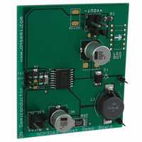
EVAL BOARD FOR NCP3163BST
Manufacturer
ON Semiconductor
Specifications of NCP3163BSTEVB
Design Resources
NCP3163 Boost Eval Board BOM NCP3163BSTEVB Gerber Files NCP3163 Boost Eval Board Schematic
Main Purpose
DC/DC, Step Up
Outputs And Type
1, Non-Isolated
Voltage - Output
24V
Current - Output
700mA
Voltage - Input
12V
Regulator Topology
Boost
Frequency - Switching
300kHz
Board Type
Fully Populated
Utilized Ic / Part
NCP3163
Lead Free Status / RoHS Status
Lead free / RoHS Compliant
Power - Output
-
Lead Free Status / Rohs Status
Lead free / RoHS Compliant
For Use With/related Products
NCP3163BST
Other names
NCP3163BSTEVBOS


The following Converter Characteristics must be chosen:
NOTES: 1. V
NOTES:
NOTES:
NOTES: 3.
(See Notes 1,2,3)
Calculation
V
V
I pk (Switch)
ripple(pp)
ripple(pp)
I L(avg)
R SC
V out
t on
t off
t on
L
C T
V
2. V
3. The calculated t
I
V
out
out
D
in
I
L
p −
operating input voltage.
−
−
−
−
−
sat
F
Nominal operating input voltage.
Desired output voltage.
Desired output current.
Desired peak−to−peak inductor ripple current. For maximum output current it is suggested that
than 10% of the average inductor current I
threshold set by R
proportionally reduce converter output current capability.
Maximum output switch frequency.
Desired peak−to−peak output ripple voltage. For best performance the ripple voltage should be kept to a low value
since it will directly affect line and load regulation. Capacitor C
electrolytic designed for switching regulator applications.
− Output rectifier forward voltage drop. Typical value for 1N5822 Schottky barrier rectifier is 0.5 V.
− Saturation voltage of the output switch, refer to Figures 10 and 11.
32.143 · 10 *6
DI L
f
V
V
on
in
in
ƒ
/t
V
I L(avg) )
* V sat * V out
8
off
ref
Step−Down
* V sat * V out
V out ) V
I pk (Switch)
ƒ
SC
t on
t
1
must not exceed the minimum guaranteed oscillator charge to discharge ratio of 8, at the minimum
off
* 20 @ 10 *12
C O
DI
. If the design goal is to use a minimum inductance value, let
t on
t
0.25
R 2
R 1
I out
off
L
) 1
2
) 1
) (ESR) 2
DI
F
2
L
t on
Figure 22. Design Equations
http://onsemi.com
L(avg)
32.143 · 10 *6
. This will help prevent I
f
11
V out ) V
V
I out
V
I L(avg) )
ƒ
ref
in
V
[
I pk (Switch)
Step−Up
in
* 20 @ 10 *12
DI
t on
t
* V sat
off
t on I out
t on
t
R 2
R 1
0.25
V sat
off
O
L
t on
t
C
off
should be a low equivalent series resistance (ESR)
F
) 1
O
) 1
) 1
V
DI
2
in
L
t on
pk (Switch)
from reaching the current limit
D
I
32.143 · 10 *6
L
= 2(I
L(avg)
f
Voltage−Inverting
I out
V
V
D
). This will
I L(avg) )
ƒ
ref
I
in
L
|V out | ) V
V
[
I pk (Switch)
be chosen to be less
in
* 20 @ 10 *12
* V sat
DI
t on
t
off
t on
t
R 2
R 1
t on I out
off
0.25
* V sat
L
t on
t
off
C
) 1
O
) 1
) 1
DI
2
F
L
t on
Related parts for NCP3163BSTEVB
Image
Part Number
Description
Manufacturer
Datasheet
Request
R

Part Number:
Description:
3.4 A, Stepup/down/inverting 50300 Khz Switching Regulator
Manufacturer:
ON Semiconductor
Datasheet:

Part Number:
Description:
EVAL BOARD FOR NCP3163INV
Manufacturer:
ON Semiconductor
Datasheet:
Part Number:
Description:
ON Semiconductor [VOLTAGE REGULATOR]
Manufacturer:
ON Semiconductor
Datasheet:
Part Number:
Description:
357-036-542-201 CARDEDGE 36POS DL .156 BLK LOPRO
Manufacturer:
ON Semiconductor
Datasheet:
Part Number:
Description:
357-036-542-201 CARDEDGE 36POS DL .156 BLK LOPRO
Manufacturer:
ON Semiconductor
Datasheet:
Part Number:
Description:
357-036-542-201 CARDEDGE 36POS DL .156 BLK LOPRO
Manufacturer:
ON Semiconductor
Datasheet:
Part Number:
Description:
357-036-542-201 CARDEDGE 36POS DL .156 BLK LOPRO
Manufacturer:
ON Semiconductor
Datasheet:
Part Number:
Description:
357-036-542-201 CARDEDGE 36POS DL .156 BLK LOPRO
Manufacturer:
ON Semiconductor
Datasheet:
Part Number:
Description:
357-036-542-201 CARDEDGE 36POS DL .156 BLK LOPRO
Manufacturer:
ON Semiconductor
Datasheet:
Part Number:
Description:
357-036-542-201 CARDEDGE 36POS DL .156 BLK LOPRO
Manufacturer:
ON Semiconductor
Datasheet:
Part Number:
Description:
357-036-542-201 CARDEDGE 36POS DL .156 BLK LOPRO
Manufacturer:
ON Semiconductor
Datasheet:
Part Number:
Description:
357-036-542-201 CARDEDGE 36POS DL .156 BLK LOPRO
Manufacturer:
ON Semiconductor
Datasheet:
Part Number:
Description:
357-036-542-201 CARDEDGE 36POS DL .156 BLK LOPRO
Manufacturer:
ON Semiconductor
Datasheet:
Part Number:
Description:
Manufacturer:
ON Semiconductor
Datasheet: