NCP5424EVB ON Semiconductor, NCP5424EVB Datasheet - Page 13
NCP5424EVB
Manufacturer Part Number
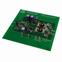
NCP5424EVB
Description
EVAL BOARD FOR NCP5424
Manufacturer
ON Semiconductor
Specifications of NCP5424EVB
Design Resources
NCP5424 Demo Board BOM NCP5424EVB Gerber Files NCP5424EVB Schematic
Main Purpose
DC/DC, Step Down
Outputs And Type
1, Non-Isolated
Voltage - Output
1.5V
Current - Output
17A
Voltage - Input
3.3V, 5V, 12V
Regulator Topology
Buck
Frequency - Switching
300kHz
Board Type
Fully Populated
Utilized Ic / Part
NCP5424
Lead Free Status / RoHS Status
Lead free / RoHS Compliant
Power - Output
-
Lead Free Status / Rohs Status
Lead free / RoHS Compliant
For Use With/related Products
NCP5424
Other names
NCP5424EVBOS


where:
MOSFET switch−on and switch−off and can be determined
by using the following formula:
where:
then be calculated as:
where:
known, the maximum FET switch junction temperature can
be calculated:
where:
Selection of the Synchronous (Lower) FET
calculated as follows:
where:
except for losses in the internal body diode, because it turns
on into near zero voltage conditions. The MOSFET body
diode will conduct during the non−overlap time and the
P HFET(TOTAL) + P RMS(H) ) P SWH(ON) ) P SWH(OFF)
P
I
R
The upper MOSFET switching losses are caused during
P
P
V
I
t
t
T = 1/f
The total power dissipation in the switching MOSFET can
P
P
P
P
Once the total power dissipation in the switching FET is
T
T
P
R
The switch conduction losses for the lower FET can be
P
I
D = Duty Cycle;
R
The synchronous MOSFET has no switching losses,
RISE
FALL
RMS(H)
OUT
OUT
RMS(H)
SWH(ON)
SWH(OFF)
HFET(TOTAL)
RMS(H)
SWH(ON)
SWH(OFF)
A
HFET(TOTAL)
RMS(L)
J
DS(ON)
qJA
DS(ON)
IN
= FET junction temperature;
= ambient temperature;
P RMS(L) + I RMS 2
= input voltage;
= upper FET junction−to−ambient thermal resistance.
= load current;
= MOSFET rise time (from FET manufacturer’s
= load current;
= MOSFET fall time (from FET manufacturer’s
SW
switching characteristics performance curve);
T J + T A ) [P HFET(TOTAL)
P SWH + P SWH(ON) ) P SWH(OFF)
= maximum switching MOSFET RMS current;
switching characteristics performance curve);
= lower MOSFET conduction losses;
P RMS(H) + I RMS(H) 2
= switching MOSFET conduction losses;
= FET drain−to−source on−resistance
= upper MOSFET switch conduction Losses;
= lower FET drain−to−source on−resistance.
= period.
= upper MOSFET switch−on losses;
= upper MOSFET switch−on losses;
= upper MOSFET switch−off losses;
= upper MOSFET switch−off losses;
+ [I OUT
= total switching (upper) MOSFET losses;
= total switching (upper) FET losses;
+
V IN
I OUT
(1 * D) ] 2
R DS(ON)
6T
(t RISE ) t FALL )
R DS(ON)
R DS(ON)
R qJA ]
http://onsemi.com
NCP5424
13
resulting power dissipation (neglecting reverse recovery
losses) can be calculated as follows:
where:
GATE(H)−to−GA TE(L) delay (from NCP5424 data sheet
Electrical Characteristics section);
MOSFET can then be calculated as:
where:
is known the maximum FET switch junction temperature
can be calculated:
where:
Control IC Power Dissipation
used, V
average MOSFET gate charge current typically dominates
the control IC power dissipation.
P CONTROL(IC) + I CC1 V CC1 ) I BST V BST ) P GATE(H)1
where:
are:
where:
losses are:
P
V
I
Non−overlap
f
The total power dissipation in the synchronous (lower)
P
P
P
Once the total power dissipation in the synchronous FET
T
T
P
R
The power dissipation of the IC varies with the MOSFETs
The IC power dissipation is determined by the formula:
P
I
V
P
P
The upper (switching) MOSFET gate driver (IC) losses
P
Q
f
The lower (synchronous) MOSFET gate driver (IC)
P SWL + V SD
LOAD
SW
CC1
SW
SWL
LFET(TOTAL)
RMS(L)
SWL
A
LFET(TOTAL)
CONTROL(IC)
GATE(H)
GATE(L)
GATE(H)
J
qJA
SD
CC1
GATE(H)
= MOSFET junction temperature;
= ambient temperature;
= switching frequency.
= switching frequency;
= lower FET source−to−drain voltage;
= IC quiescent supply current;
= lower FET junction−to−ambient thermal resistance.
CC
= IC supply voltage;
= lower FET switching losses;
= Switching losses.
P GATE(H) + Q GATE(H)
P GATE(L) + Q GATE(L)
= load current;
T J + T A ) [P LFET(TOTAL)
P LFET(TOTAL) + P RMS(L) ) P SWL
, and the NCP5424 operating frequency. The
= Switch Conduction Losses;
= lower MOSFET gate driver (IC) losses.
= upper MOSFET gate driver (IC) losses;
= upper MOSFET gate driver (IC) losses;
= total upper MOSFET gate charge at V
) P GATE(L)1 ) P GATE(H)2 ) P GATE(L)2
= Synchronous (lower) FET total losses;
= total synchronous (lower) FET losses;
= control IC power dissipation;
time
I LOAD
=
GATE(L)−to−GA TE(H)
non−overlap time
f SW
f SW
R qJA ]
V CC
V BST
f SW
CC
;
or
Related parts for NCP5424EVB
Image
Part Number
Description
Manufacturer
Datasheet
Request
R

Part Number:
Description:
Dual Synchronous Buck Controller
Manufacturer:
ON Semiconductor
Datasheet:
Part Number:
Description:
ON Semiconductor [VOLTAGE REGULATOR]
Manufacturer:
ON Semiconductor
Datasheet:
Part Number:
Description:
357-036-542-201 CARDEDGE 36POS DL .156 BLK LOPRO
Manufacturer:
ON Semiconductor
Datasheet:
Part Number:
Description:
357-036-542-201 CARDEDGE 36POS DL .156 BLK LOPRO
Manufacturer:
ON Semiconductor
Datasheet:
Part Number:
Description:
357-036-542-201 CARDEDGE 36POS DL .156 BLK LOPRO
Manufacturer:
ON Semiconductor
Datasheet:
Part Number:
Description:
357-036-542-201 CARDEDGE 36POS DL .156 BLK LOPRO
Manufacturer:
ON Semiconductor
Datasheet:
Part Number:
Description:
357-036-542-201 CARDEDGE 36POS DL .156 BLK LOPRO
Manufacturer:
ON Semiconductor
Datasheet:
Part Number:
Description:
357-036-542-201 CARDEDGE 36POS DL .156 BLK LOPRO
Manufacturer:
ON Semiconductor
Datasheet:
Part Number:
Description:
357-036-542-201 CARDEDGE 36POS DL .156 BLK LOPRO
Manufacturer:
ON Semiconductor
Datasheet:
Part Number:
Description:
357-036-542-201 CARDEDGE 36POS DL .156 BLK LOPRO
Manufacturer:
ON Semiconductor
Datasheet:
Part Number:
Description:
357-036-542-201 CARDEDGE 36POS DL .156 BLK LOPRO
Manufacturer:
ON Semiconductor
Datasheet:
Part Number:
Description:
357-036-542-201 CARDEDGE 36POS DL .156 BLK LOPRO
Manufacturer:
ON Semiconductor
Datasheet:
Part Number:
Description:
Manufacturer:
ON Semiconductor
Datasheet:
Part Number:
Description:
Manufacturer:
ON Semiconductor
Datasheet: