NCP5424EVB ON Semiconductor, NCP5424EVB Datasheet
NCP5424EVB
Specifications of NCP5424EVB


Related parts for NCP5424EVB

NCP5424EVB Summary of contents
Page 1
... DDR Memory High Current (Two−Phase) Power Supplies Dual Output DC−DC Converters *For additional information on our Pb−Free strategy and soldering details, please download the ON Semiconductor Soldering and Mounting Techniques Reference Manual, SOLDERRM/D. Semiconductor Components Industries, LLC, 2005 March, 2005 − Rev. 4 http://onsemi ...
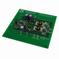
Page 2
V 5 220 mF 220 MTD60N03 1.3 mH/15 A C3/4 680 mF/ MTD90N02 ...
Page 3
MAXIMUM RATINGS Operating Junction Temperature Storage Temperature Range ESD Susceptibility (Human Body Model) Package Thermal Resistance, SOIC−16: Lead Temperature Soldering: Maximum ratings are those values beyond which device damage can occur. Maximum ratings applied to the ...
Page 4
ELECTRICAL CHARACTERISTICS 10.8 V < V < 13.2 V; 10.8 V < BST < Characteristic Error Amplifier V Bias Current FB V Input Range FB1(2) COMP1,2 Source Current COMP1,2 Sink Current Reference Voltage 1(2) COMP1,2 Max ...
Page 5
ELECTRICAL CHARACTERISTICS (continued) 10.8 V < V < 13.2 V; 10.8 V < BST < Characteristic Oscillator Switching Frequency Switching Frequency Switching Frequency R Voltage OSC Phase Difference Supply Currents V Current CC BST Current Undervoltage ...
Page 6
BIAS V CC 8.6 V 7.8 V IS+1 IS− IS+2 FAULT Set Dominant R 0. 1.0 V NCP5424 OSC CURRENT SOURCE GEN CLK1 OSC CLK2 PWM Comparator 1 ...
Page 7
THEORY OF OPERATION The NCP5424 is a dual output or single two−phase power 2 supply controller that utilizes the V 2 synchronous V buck regulators can be built using a single controller or a single output converter that draws programmable ...
Page 8
PWM pulse. This pulse will gradually increase in width as the voltage ramp on the Compensation Capacitor continues to rise. This process will continue until the output voltage reaches the designed value set by the feed back ...
Page 9
Out−of−Phase Synchronization In out−of−phase synchronization, the turn−on of the second channel is delayed by half the switching cycle. This delay is supervised by the oscillator, which supplies a clock signal to the second channel which is 180 out of phase ...
Page 10
DESIGN GUIDELINES Definition of the design specifications The output voltage tolerance can be affected by any or all of the following: 1. buck regulator output voltage setpoint accuracy; 2. output voltage change due to discharging or charging of the bulk ...
Page 11
Powdered iron cores are very suitable due to its high saturation flux density and have low loss at high frequencies, a distributed gap and exhibit very low EMI. The minimum value of inductance which prevents inductor saturation or ...
Page 12
The actual output voltage deviation due to ESR can then be verified and compared to the value assigned by the designer: DV ESR + DI OUT ESR MAX Similarly, the maximum allowable ESL is calculated from the following formula: DV ...
Page 13
P RMS( RMS( DS(ON) where switching MOSFET conduction losses; RMS( maximum switching MOSFET RMS current; RMS( FET drain−to−source on−resistance DS(ON) The upper MOSFET switching losses are caused during MOSFET switch−on ...
Page 14
P = lower MOSFET gate driver (IC) losses; GATE( total lower MOSFET gate charge at V GATE( switching frequency; SW The junction temperature of the control IC is primarily a function of the PCB layout, ...
Page 15
Comp1 pin and a 0.01 mF capacitor on the Comp2 pin in suggested. Selecting Current Sharing Current Limit In a two−phase single output application, there are two different current limit options. The Master (Controller One) current limit ...
Page 16
R SENSE + 0.070 V I LIMIT In a high current supply, the sense resistor will be a very low value, typically less than 10 mW. Such a resistor can be either a discrete component or a PCB trace. The ...
Page 17
EMI MANAGEMENT As a consequence of large currents being turned on and off at high frequency, switching regulators generate noise as a consequence of their normal operation. When designing for compliance with EMI/EMC regulations, additional components may be added to ...
Page 18
... American Technical Support: 800−282−9855 Toll Free USA/Canada Japan: ON Semiconductor, Japan Customer Focus Center 2−9−1 Kamimeguro, Meguro−ku, Tokyo, Japan 153−0051 Phone: 81−3−5773−3850 http://onsemi.com 18 NOTES: 1. DIMENSIONING AND TOLERANCING PER ANSI Y14.5M, 1982. 2. CONTROLLING DIMENSION: MILLIMETER. ...