STEVAL-ISA029V1 STMicroelectronics, STEVAL-ISA029V1 Datasheet - Page 20
STEVAL-ISA029V1
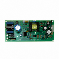
Manufacturer Part Number
STEVAL-ISA029V1
Description
BOARD EVAL BASED ON VIPER53-E
Manufacturer
STMicroelectronics
Series
VIPER™r
Type
MOSFET & Power Driverr
Specifications of STEVAL-ISA029V1
Design Resources
STEVAL-ISA029V1 Gerber Files STEVAL-ISA029V1 Schematic STEVAL-ISA029V1 Bill of Material
Main Purpose
AC/DC, Primary Side
Outputs And Type
3, Isolated
Power - Output
13W
Voltage - Output
12V, 3.3V, -24V
Current - Output
1A, 100mA, 40mA
Voltage - Input
85 ~ 300VAC
Regulator Topology
Flyback
Frequency - Switching
60kHz
Board Type
Fully Populated
Utilized Ic / Part
VIPer53
Input Voltage
85 V to 300 V
Output Voltage
12 V
Product
Power Management Modules
Silicon Manufacturer
ST Micro
Silicon Core Number
VIPer53-E
Kit Application Type
Power Management
Application Sub Type
Power Supply
Kit Contents
Board
Rohs Compliant
No
Lead Free Status / RoHS Status
Lead free / RoHS Compliant
For Use With/related Products
VIPer53-E
Other names
497-6458
STEVAL-ISA029V1
STEVAL-ISA029V1


Standby mode
8
20/36
Standby mode
The device offers a special feature to address the low load condition. The corresponding
function described hereafter consists of reducing the switching frequency by going into burst
mode, with the following benefits:
For this purpose, a comparator monitores the COMP pin voltage, and maintains the PWM
latch and the Power MOSFET in the Off state as long as V
Block Diagram
the minimum turn on of the device, the V
0.5V threshold (V
resumes normal operation as soon as V
regulated in burst mode. The corresponding ripple is not higher than the nominal one at full
load.
In addition, the minimum turn on time which defines the frontier between normal operation
and burst mode changes according to V
time increases to 400ns, whereas for higher voltages, it is 150ns
minimum turn on times resulting from these values are respectively 600 ns and 350 ns,
when taking into account internal propagation time. This brutal change induces an
hysteresis between normal operation and burst mode as shown on
When the output power decreases, the system reaches point 2 where V
V
the effective turn-on time that should be needed at this output power level. Therefore the
regulation loop will quickly drive V
mode and to control the output voltage. The corresponding hysteresis can be seen on the
switching frequency which passes from F
by the components connected to the OSC pin and to FSWstby. Note: This frequency is
actually an equivalent number of switching pulses per second, rather than a fixed switching
frequency since the device is working in burst mode.
As long as the power remains below P
V
missing cycles decreases) as the power approaches P
operation at point 1. The hysteresis cannot be seen on the switching frequency, but it can be
seen in the sudden surge of the COMP pin voltage from point 3 to point 1 at that power level.
The power points value P
Equation 2
COMPbl
COMPsd
– It reduces the switching losses, thus providing low consumption on the mains lines.
– It allows the regulation of the output voltage, even if the load corresponds to a duty
The device is compliant with “Blue Angel” and other similar standards, requiring less
than 0.5 W of input power when in standby.
cycle that the device is not able to generate because of the internal blanking time, and
associated minimum turn on.
. The minimum turn-on time passes immediately from 350ns to 600ns, exceeding
and the converter works in burst mode. Its “density” increases (i.e. the number of
on page
COMPoff
1). If the output load requires a duty cycle below the one defined by
). The Power MOSFET can be completely Off for some cycles, and
P
RST
RST
and P
=
1
-- -
2
COMP
STBY
F
SWnom
RST
to V
COMP
COMP
COMP
SWnom
are defined by the following formulas:
the output of the regulation loop remains stuck at
COMPoff
value. Below 1.0V (V
is higher than 0.5V. The output voltage is
net decreases its voltage until it reaches this
tb
which is the normal switching frequency set
1
+
td
(Point 3) in order to pass into burst
2
RST
V
COMP
and finally resumes normal
2
IN
------ -
Lp
remains below 0.5V (See
1
Figure 6 on page 10
COMPbl
Figure 20 on page
COMP
), the blanking
equals
VIPer53 - E
The
21.
Related parts for STEVAL-ISA029V1
Image
Part Number
Description
Manufacturer
Datasheet
Request
R

Part Number:
Description:
BOARD RGB CTR ST7,STP08C596MTR
Manufacturer:
STMicroelectronics
Datasheet:

Part Number:
Description:
Power Management IC Development Tools Full Speed USB to RS232 Bridge Demo
Manufacturer:
STMicroelectronics
Datasheet:
Part Number:
Description:
Power Management IC Development Tools 2.5W solar eval BRD USB SPV1040 LD39050
Manufacturer:
STMicroelectronics
Datasheet:

Part Number:
Description:
BOARD EVAL FOR MEMS SENSORS
Manufacturer:
STMicroelectronics
Datasheet:

Part Number:
Description:
KIT DEV STARTER ST10F276Z5
Manufacturer:
STMicroelectronics
Datasheet:

Part Number:
Description:
BOARD EVAL HDMI $ VIDEO SWITCH
Manufacturer:
STMicroelectronics
Datasheet:

Part Number:
Description:
BOARD DEMO ACCELEROMETER DIL24
Manufacturer:
STMicroelectronics
Datasheet:

Part Number:
Description:
BOARD STLM75/STDS75/ST72F651
Manufacturer:
STMicroelectronics
Datasheet:

Part Number:
Description:
EVAL BOARD 3AXIS MEMS ACCELLRMTR
Manufacturer:
STMicroelectronics
Datasheet:

Part Number:
Description:
BOARD EVAL 8BIT MICRO + TDE1708
Manufacturer:
STMicroelectronics
Datasheet:
Part Number:
Description:
STMicroelectronics [RIPPLE-CARRY BINARY COUNTER/DIVIDERS]
Manufacturer:
STMicroelectronics
Datasheet:
Part Number:
Description:
STMicroelectronics [LIQUID-CRYSTAL DISPLAY DRIVERS]
Manufacturer:
STMicroelectronics
Datasheet:
Part Number:
Description:
BOARD EVAL FOR MEMS SENSORS
Manufacturer:
STMicroelectronics
Datasheet: