STEVAL-PSQ001V1 STMicroelectronics, STEVAL-PSQ001V1 Datasheet
STEVAL-PSQ001V1
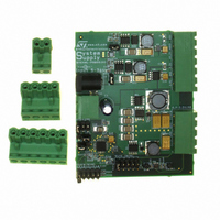
Specifications of STEVAL-PSQ001V1
STEVAL-PSQ001V1


Related parts for STEVAL-PSQ001V1


STEVAL-PSQ001V1 Summary of contents
Page 1
Features ■ input voltage range ■ Adjustable output voltages ■ 5V LDO delivers 100 mA peak current ± ■ 1.237 reference voltage available externally ■ Current sensing using low side MOSFETs R ...
Page 2
Contents Contents 1 Block diagram . . . . . . . . . . . . . . . . . . . . . . . . . . . . . . . . . . . ...
Page 3
PM6680A 9 Design guidelines . . . . . . . . . . . . . . . . . . . . . . . . . . . . . . . . . . . . ...
Page 4
Block diagram 1 Block diagram Figure 1. Functional block diagram V CC VREF NC FB2 OUT2 SKIP FREQUENCY FSEL SELECTOR BOOT2 HGATE2 PHASE2 COMP2 LDO5 LGATE2 SHDN EN2 4/48 VIN 5V REFERENCE VREF LINEAR GENERATOR REGULATOR LDO5 ENABLE LEVEL OUT2 ...
Page 5
PM6680A 2 Pin settings 2.1 Connections Figure 2. Pin connection (through top view) 1 PM6680A Pin settings 5/48 ...
Page 6
Pin settings 2.2 Functions Table 2. Pin functions N° Pin Signal ground. Reference for internal logic circuitry. It must be connected to the 1 SGND1 signal ground plan of the power supply. The signal ground plan and the power ground ...
Page 7
PM6680A Table 2. Pin functions (continued) N° Pin Internal 5 V regulator bypass connection. • If V5SW is connected to OUT5 ( external 5 V supply) and V5SW is greater 17 V5SW than 4.9 V, the LDO5 regulator ...
Page 8
Electrical data 3 Electrical data 3.1 Maximum rating Table 3. Absolute maximum ratings V5SW, LDO5 to PGND VIN to PGND HGATEx and BOOTx, to PHASEx PHASEx to PGND CSENSEx , to PGND CSENSEx to BOOTx LGATEx to PGND FBx, COMPx, ...
Page 9
PM6680A 4 Electrical characteristics Table 5. Electrical characteristics T = -40 °C to 125 °C, unless otherwise specified. All parameters at operating temperature A extremes are guaranteed by design and statistical analysis (not production tested). Symbol Parameter Supply section VIN ...
Page 10
Electrical characteristics Table 5. Electrical characteristics (continued -40 °C to 125 °C, unless otherwise specified. All parameters at operating temperature A extremes are guaranteed by design and statistical analysis (not production tested). Symbol Parameter Minimum on time On ...
Page 11
PM6680A Table 5. Electrical characteristics (continued -40 °C to 125 °C, unless otherwise specified. All parameters at operating temperature A extremes are guaranteed by design and statistical analysis (not production tested). Symbol Parameter High and low gate drivers ...
Page 12
Typical operating characteristics 5 Typical operating characteristics FSEL=GND(200/300 kHz), SKIP=GND(skip mode), V5SW=EXT5V (external 5 V power supply connected), input voltage VIN = 24 V, SHDN, EN1 and EN2 high, OUT1 = 3.3 V, OUT2 = 1 load unless ...
Page 13
PM6680A Figure 7. No-audible skip no load battery current vs input voltage Figure 9. Shutdown mode input battery current vs input voltage Figure 11. OUT1 = 3.3 V switching frequency Typical operating characteristics Figure 8. Standby mode input battery current ...
Page 14
Typical operating characteristics Figure 13. OUT1 = 3.3 V load regulation Figure 15. Voltage reference vs load current Figure 17. OUT1 = 3.3V load transient 0 14/48 Figure 14. OUT2 = 1.8 V load regulation Figure 16. OUT1, OUT2 and ...
Page 15
PM6680A Figure 19. 3.3 V soft start (1Ω load) Figure 21. OUT1 = 3.3 V soft end (no load) Figure 23. OUT1 = 3.3 V soft end (0.8 load) Typical operating characteristics Figure 20. 1.8 V soft start (0.6Ω load) ...
Page 16
Typical operating characteristics Figure 25. 3.3 V no-audible skip mode 16/48 Figure 26. 1.8 V no-audible skip mode PM6680A ...
Page 17
PM6680A 6 Application schematic Figure 27. Simplified application schematic VIN 19 LDO5 18 VCC ...
Page 18
Device description 7 Device description The PM6680A is a dual step-down controller dedicated to provide logic voltages for industrial automation applications based on a Constant On Time control architecture. This type of control offers a very fast load ...
Page 19
PM6680A Figure 28. Constant ON time PWM control The duty cycle of the buck converter in steady state is: Equation 2 The PWM control works at a nearly fixed frequency f Equation 3 As mentioned the steady state switching frequency ...
Page 20
Device description 7.2 Constant on time architecture Figure 29 shows the simplified block diagram of a constant on time controller. A minimum off-time constrain (350 ns typ.) is introduced to allow inductor valley current sensing on synchronous switch. A minimum ...
Page 21
PM6680A 7.3 Output ripple compensation and loop stability In a classic constant on time control, the system regulates the valley value of the output voltage and not the average value, as shown in voltage ripple is source ...
Page 22
Device description 7.4 Pulse skip mode If the SKIP pin is tied to ground, the device works in skip mode. At light loads a zero-crossing comparator truncates the low-side switch on-time when the inductor current becomes negative. In this condition ...
Page 23
PM6680A 7.5 No-audible skip mode If SKIP pin is tied kHz is enabled. At light load condition, If there is not a new switching cycle within a 30 µs (typ.) period, a no-audible skip mode cycle begins. ...
Page 24
Device description 7.6 Current limit The current-limit circuit employs a "valley" current-sensing algorithm. During the conduction time of the low side MOSFET the current flowing through it is sensed. The current-sensing element is the low side MOSFET on-resistance Figure 33. ...
Page 25
PM6680A Being fixed the valley threshold, the greater the current ripple is, greater the DC output current is The valley current limit can be set with resistor RCSENSE: Equation 7 = 100 µA, RDSon is the drain-source on resistance of ...
Page 26
Device description Figure 35. Soft start waveforms When a switching section is turned off (EN1/EN2 pins low), the controller enters in soft end mode.The output capacitor is discharged through an internal 18 Ω p-MOSFET switch; when the output voltage reaches ...
Page 27
PM6680A 7.9 Reference voltage and bandgap The 1.237 V (typ.) internal bandgap voltage is accurate to ±1 % over the temperature range externally available (VREF pin) and can supply up to ± 100 µA and can be used ...
Page 28
Device description 7.11 Power up sequencing and operative modes Let us consider SHDN, EN1 and EN2 low at the beginning. An external voltage is applied as input voltage. The device is in shutdown mode. When the SHDN pin voltage is ...
Page 29
PM6680A 8 Monitoring and protections Power good signals The PM6680A provides two independent power good signals: one for each switching section (PGOOD1/PGOOD2). PGOOD1/PGOOD2 signals are low if the output voltage is out of ± the designed set ...
Page 30
Design guidelines 9 Design guidelines The design of a switching section starts from two parameters: ● Input voltage range: in notebook applications it varies from the minimum battery voltage, VINmin to the AC adapter voltage, V ● Maximum load current: ...
Page 31
PM6680A Equation 14 If hard saturation inductors are used, the inductor saturation current should be much greater than the maximum inductor peak current Ipeak: Equation 15 Using soft saturation inductors it's possible to choose inductors with saturation current limit nearly ...
Page 32
Design guidelines Table 11. Output capacitor manufacturer Manufacturer SANYO PANASONIC 9.4 Input capacitors selection In a buck topology converter the current that flows into the input capacitor is a pulsed current with zero average value. The input RMS current of ...
Page 33
PM6680A 9.5 Power MOSFETS Logic-level MOSFETs are recommended, since low side and high side gate drivers are powered by LDO5. Their breakdown voltage VBR In notebook applications, power management efficiency is a high level requirement. The power dissipation on the ...
Page 34
Design guidelines Equation 22 Choose a synchronous rectifier with low R variation of the phase node voltage can bring up even the low side gate through its gate- drain capacitance C that minimizes the ratio C Below there is a ...
Page 35
PM6680A 9.6 Closing the integrator loop The design of external feedback network depends on the output voltage ripple. If the ripple is higher than approximately 30 mV, the feedback network ( keep the loop stable. Figure 36. Circuitry for output ...
Page 36
Design guidelines In order to ensure stability it must be also verified that: Equation 25 In order to reduce ground noise due to load transient on the other section recommended to add a resistor R low pass filter ...
Page 37
PM6680A Figure 37. Virtual ESR network ∆V ∆V Output Output voltage voltage ∆V ∆ The T node voltage is the sum of the output voltage and the triangular waveform generated by the virtual ESR network. In ...
Page 38
Design guidelines Equation 30 where R is the sum of the ESR of the output capacitor R TOT by the virtual ESR network RESR. Moreover C must meet the following condition: INT Equation 31 Where free design ...
Page 39
PM6680A 9.7 Other parts design ● VIN filter A VIN pin low pass filter is suggested to reduce switching noise. The low pass filter is shown in the next figure: Figure 38. VIN pin filter Typical components values are: R ...
Page 40
Design guidelines Figure 40. Bootstrap circuit The bootstrap circuit capacitor value C side MOSFET during turn on phase. A typical value is 100 nF. The bootstrap diode D must charge the capacitor during the off time phases. The maximum rated ...
Page 41
PM6680A Equation 37 We choose standard value L=4.7 µH. ∆I = 0.886 A @VIN =24 V. L(max 2.523 A LRMS 3.83 A peak 2. Output capacitor selection We would like ...
Page 42
Design guidelines Equation 41 (Let's assume Tmax=75 ° 560 Ω. R CSENSE 5. Input capacitor Maximum input capacitor RMS current is about 1.084 A. Then I We put two 10 µF ceramic capacitors with Irms = 1.5 ...
Page 43
PM6680A Figure 41. Current paths, ground connection and driver traces layout Design guidelines 43/48 ...
Page 44
Design guidelines ● As general rule, make the high side and low side drivers traces wide and short. The high side driver is powered by the bootstrap circuit. It's very important to place capacitor CBOOT and diode DBOOT as near ...
Page 45
PM6680A 10 Package mechanical data In order to meet environmental requirements, ST offers these devices in ECOPACK packages. These packages have a Lead-free second level interconnect. The category of second Level Interconnect is marked on the package and on the ...
Page 46
Package mechanical data Figure 42. Package dimensions 46/48 PM6680A ...
Page 47
PM6680A 11 Revision history Table 18. Document revision history Date 12-Oct-2006 17-Dec-2007 Revision 1 Initial release. Added Section 5: Typical operating characteristics on page 12 2 Section 9: Design guidelines on page 30 Revision history Changes and 47/48 ...
Page 48
... Information in this document is provided solely in connection with ST products. STMicroelectronics NV and its subsidiaries (“ST”) reserve the right to make changes, corrections, modifications or improvements, to this document, and the products and services described herein at any time, without notice. All ST products are sold pursuant to ST’s terms and conditions of sale. ...