STEVAL-ISA052V1 STMicroelectronics, STEVAL-ISA052V1 Datasheet - Page 38
STEVAL-ISA052V1
Manufacturer Part Number
STEVAL-ISA052V1
Description
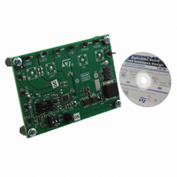
KIT EVAL PM6675S HE CTLR 2A REG
Manufacturer
STMicroelectronics
Specifications of STEVAL-ISA052V1
Main Purpose
DC/DC, Step Down with LDO
Outputs And Type
2, Non-Isolated
Voltage - Output
1.5V, 0.6 ~ 3.3V
Current - Output
10A, 2A
Voltage - Input
4.5 ~ 28 V
Regulator Topology
Buck
Board Type
Fully Populated
Utilized Ic / Part
PM6675
Product
Power Management Modules
Lead Free Status / RoHS Status
Lead free / RoHS Compliant
Power - Output
-
Frequency - Switching
-
Lead Free Status / Rohs Status
Lead free / RoHS Compliant
Other names
497-8426
Available stocks
Company
Part Number
Manufacturer
Quantity
Price
Company:

Part Number:
STEVAL-ISA052V1
Manufacturer:
STMicroelectronics
Quantity:
1


Application information
8
8.1
38/53
Application information
The purpose of this chapter is showing the design procedure of the switching section.
The design starts from three main specifications:
●
●
●
It's also possible that specific designs should involve other specifications.
The following paragraphs will guide the user into a step-by-step design.
External components selection
The PM6675S uses a pseudo-fixed frequency, Constant On-Time (COT) controller as the
core of the switching section. The switching frequency can be set by connecting an external
divider to the VOSC pin. The voltage seen at this pin must be greater than 0.8V and lower
than 2 V in order to ensure system linearity.
Nearly constant switching frequency is achieved by the system loop in steady-state
operating conditions by varying the On-Time duration, avoiding thus the need for a clock
generator. The On-Time one shot duration is directly proportional to the output voltage,
sensed at VSNS pin, and inversely proportional to the input voltage, sensed at the VOSC
pin, as follows:
Equation 25
where K
(40 ns typ.).
The duty cycle of the buck converter is, in under steady state conditions, given by
Equation 26
The switching frequency is thus calculated as
Equation 27
The input voltage range, provided by the battery or the external supply. The two
extreme values (V
The maximum load current, indicated with I
The maximum allowed output voltage ripple V
OSC
is a constant value (130 ns typ.) and τ is the internal propagation delay
INMAX
f
SW
and V
=
T
D
ON
INmin
T
=
ON
K
=
OSC
) are important for the design.
D =
K
V
V
OSC
OUT
⋅
IN
V
V
V
V
OUT
OSC
SNS
IN
V
V
LOAD,MAX
OSC
SNS
RIPPLE,MAX
=
+
α
α
τ
OSC
OUT
.
⋅
K
.
OSC
1
PM6675S
Related parts for STEVAL-ISA052V1
Image
Part Number
Description
Manufacturer
Datasheet
Request
R

Part Number:
Description:
BOARD RGB CTR ST7,STP08C596MTR
Manufacturer:
STMicroelectronics
Datasheet:

Part Number:
Description:
Power Management IC Development Tools Full Speed USB to RS232 Bridge Demo
Manufacturer:
STMicroelectronics
Datasheet:
Part Number:
Description:
Power Management IC Development Tools 2.5W solar eval BRD USB SPV1040 LD39050
Manufacturer:
STMicroelectronics
Datasheet:

Part Number:
Description:
BOARD EVAL FOR MEMS SENSORS
Manufacturer:
STMicroelectronics
Datasheet:

Part Number:
Description:
KIT DEV STARTER ST10F276Z5
Manufacturer:
STMicroelectronics
Datasheet:

Part Number:
Description:
BOARD EVAL HDMI $ VIDEO SWITCH
Manufacturer:
STMicroelectronics
Datasheet:

Part Number:
Description:
BOARD DEMO ACCELEROMETER DIL24
Manufacturer:
STMicroelectronics
Datasheet:

Part Number:
Description:
BOARD STLM75/STDS75/ST72F651
Manufacturer:
STMicroelectronics
Datasheet:

Part Number:
Description:
EVAL BOARD 3AXIS MEMS ACCELLRMTR
Manufacturer:
STMicroelectronics
Datasheet:

Part Number:
Description:
BOARD EVAL 8BIT MICRO + TDE1708
Manufacturer:
STMicroelectronics
Datasheet:
Part Number:
Description:
STMicroelectronics [RIPPLE-CARRY BINARY COUNTER/DIVIDERS]
Manufacturer:
STMicroelectronics
Datasheet:
Part Number:
Description:
STMicroelectronics [LIQUID-CRYSTAL DISPLAY DRIVERS]
Manufacturer:
STMicroelectronics
Datasheet:
Part Number:
Description:
BOARD EVAL FOR MEMS SENSORS
Manufacturer:
STMicroelectronics
Datasheet: