STEVAL-ISA027V1 STMicroelectronics, STEVAL-ISA027V1 Datasheet - Page 16
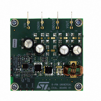
STEVAL-ISA027V1
Manufacturer Part Number
STEVAL-ISA027V1
Description
BOARD EVAL 1PH STPDN CONV L6726A
Manufacturer
STMicroelectronics
Type
DC/DC Switching Converters, Regulators & Controllersr
Specifications of STEVAL-ISA027V1
Design Resources
STEVAL-ISA027V1 Gerber Files STEVAL-ISA027V1 Schematic STEVAL-ISA027V1 Bill of Material
Main Purpose
DC/DC, Step Down
Outputs And Type
1, Non-Isolated
Voltage - Output
1.25V
Current - Output
20A
Voltage - Input
5 ~ 12V
Regulator Topology
Buck
Frequency - Switching
270kHz
Board Type
Fully Populated
Utilized Ic / Part
L6726A
Input Voltage
5 V to 12 V
Output Voltage
1.25 V
Product
Power Management Modules
Lead Free Status / RoHS Status
Lead free / RoHS Compliant
Power - Output
-
Lead Free Status / Rohs Status
Lead free / RoHS Compliant
For Use With/related Products
L6726A
Other names
497-6259


Application details
16/35
depending on the output capacitor ESR. The DC gain of the modulator is simply the input
voltage V
V
The compensation network closes the loop joining FB and COMP node with transfer
function ideally equal to -gm
Compensation goal is to close the control loop assuring high DC regulation accuracy, good
dynamic performances and stability. To achieve this, the overall loop needs high DC gain,
high bandwidth and good phase margin.
High DC gain is achieved giving an integrator shape to compensation network transfer
function. Loop bandwidth (F
should not exceed F
cross 0 dB axis with -20 dB/decade slope.
As an example,
Figure 9.
●
●
compensation
open loop
closed loop
OUT
open loop
converter
OTA
gain
gain
gain
Open loop converter singularities:
a)
b)
Compensation Network singularities frequencies:
a)
b)
gain
is scaled and transferred to FB node by the output resistor divider.
Gain
[dB]
IN
0dB
F
divided by the peak-to-peak oscillator voltage ΔV
F
LC
F
Example of type II compensation.
F
P
ESR
Z
=
=
Figure 9
=
--------------------------------- -
2π L C
------------------------------------------------- -
2π R
=
------------------------------
2π R
SW
------------------------------------------- -
2π C
⋅
⋅
/2π. To achieve a good phase margin, the control loop gain has to
1
1
⋅
⋅
F
F
F
shows an asymptotic bode plot of a type II compensation.
⋅
Z
⋅
OUT
1
⎛
⎝
OUT
C
-------------------- -
C
C
1
0dB
·
F
F
Z
F
+
Doc ID 12754 Rev 4
F
⋅
⋅
F
) can be fixed choosing the right R
ESR
.
C
LC
C
P
P
⎞
⎠
F
ESR
F
0dB
F
P
OSC
20log (gm·R
20log [V
.
F
; however, for stability, it
IN
Log (Freq)
/ΔV
F
)
OSC
·R
OS
/(R
L6726A
FB
+R
OS
)]
Related parts for STEVAL-ISA027V1
Image
Part Number
Description
Manufacturer
Datasheet
Request
R

Part Number:
Description:
BOARD RGB CTR ST7,STP08C596MTR
Manufacturer:
STMicroelectronics
Datasheet:

Part Number:
Description:
Power Management IC Development Tools Full Speed USB to RS232 Bridge Demo
Manufacturer:
STMicroelectronics
Datasheet:
Part Number:
Description:
Power Management IC Development Tools 2.5W solar eval BRD USB SPV1040 LD39050
Manufacturer:
STMicroelectronics
Datasheet:

Part Number:
Description:
BOARD EVAL FOR MEMS SENSORS
Manufacturer:
STMicroelectronics
Datasheet:

Part Number:
Description:
KIT DEV STARTER ST10F276Z5
Manufacturer:
STMicroelectronics
Datasheet:

Part Number:
Description:
BOARD EVAL HDMI $ VIDEO SWITCH
Manufacturer:
STMicroelectronics
Datasheet:

Part Number:
Description:
BOARD DEMO ACCELEROMETER DIL24
Manufacturer:
STMicroelectronics
Datasheet:

Part Number:
Description:
BOARD STLM75/STDS75/ST72F651
Manufacturer:
STMicroelectronics
Datasheet:

Part Number:
Description:
EVAL BOARD 3AXIS MEMS ACCELLRMTR
Manufacturer:
STMicroelectronics
Datasheet:

Part Number:
Description:
BOARD EVAL 8BIT MICRO + TDE1708
Manufacturer:
STMicroelectronics
Datasheet:
Part Number:
Description:
STMicroelectronics [RIPPLE-CARRY BINARY COUNTER/DIVIDERS]
Manufacturer:
STMicroelectronics
Datasheet:
Part Number:
Description:
STMicroelectronics [LIQUID-CRYSTAL DISPLAY DRIVERS]
Manufacturer:
STMicroelectronics
Datasheet:
Part Number:
Description:
BOARD EVAL FOR MEMS SENSORS
Manufacturer:
STMicroelectronics
Datasheet: