STEVAL-ISA026V1 STMicroelectronics, STEVAL-ISA026V1 Datasheet - Page 16
STEVAL-ISA026V1
Manufacturer Part Number
STEVAL-ISA026V1
Description
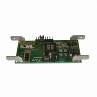
EVAL BOARD 20A 250KHZ L6732
Manufacturer
STMicroelectronics
Type
DC/DC Switching Converters, Regulators & Controllersr
Specifications of STEVAL-ISA026V1
Design Resources
STEVAL-ISA026V1 Gerber Files STEVAL-ISA026V1 Schematic STEVAL-ISA026V1 Bill of Material
Main Purpose
DC/DC, Step Down
Outputs And Type
1, Non-Isolated
Voltage - Output
3.3V
Current - Output
20A
Voltage - Input
4.5 ~ 14V
Regulator Topology
Buck
Frequency - Switching
250kHz
Board Type
Fully Populated
Utilized Ic / Part
L6732
Input Voltage
4.5 V to 14 V
Output Voltage
3.3 V
Product
Power Management Modules
Silicon Manufacturer
ST Micro
Silicon Core Number
L6732
Kit Application Type
Power Management - Voltage Regulator
Rohs Compliant
No
Lead Free Status / RoHS Status
Lead free / RoHS Compliant
Power - Output
-
Lead Free Status / Rohs Status
Lead free / RoHS Compliant
For Use With/related Products
L6732
Other names
497-5869
Available stocks
Company
Part Number
Manufacturer
Quantity
Price
Company:

Part Number:
STEVAL-ISA026V1
Manufacturer:
STMicroelectronics
Quantity:
135


Device description
5.7
5.8
16/37
Driver section
The high-side and low-side drivers allow using different types of power MOSFETs (also
multiple MOSFETs to reduce the R
The low-side driver is supplied by V
pin. A predictive dead time control avoids MOSFETs cross-conduction maintaining very
short dead time duration in the range of 20 ns. The control monitors the phase node in order
to sense the low-side body diode recirculation. If the phase node voltage is less than a
certain threshold (-350 mV typ.) during the dead time, it will be reduced in the next PWM
cycle. The predictive dead time control doesn't work when the high-side body diode is
conducting because the phase node doesn't go negative. This situation happens when the
converter is sinking current for example and, in this case, an adaptive dead time control
operates.
Monitoring and protections
The output voltage is monitored by means of pin FB. If it is not within ±10 % (typ.) of the
programmed value, the Power good (PGOOD) output is forced low.
The device provides over-voltage-protection: when the voltage sensed on FB pin reaches a
value 20% (typ.) greater than the reference, the low-side driver is turned on as long as the
over voltage is detected (see
Figure 10. OVP
It must be taken into account that there is an electrical network between the output terminal
and the FB pin and therefore the voltage at the pin is not a perfect replica of the output
voltage. However due to the fact that the converter can sink current, in the most of cases the
low-side will turn-on before the output voltage exceeds the over-voltage threshold, because
the error amplifier will throw off balance in advance. Even if the device doesn't report an
over-voltage, the behavior is the same, because the low-side is turned-on immediately. The
following figure shows the device behavior during an over-voltage event. The output voltage
Figure
DS(on)
CCDR
10.).
while the high-side driver is supplied by the BOOT
maintaining fast switching transitions.
LGate
FB
L6732
Related parts for STEVAL-ISA026V1
Image
Part Number
Description
Manufacturer
Datasheet
Request
R

Part Number:
Description:
BOARD RGB CTR ST7,STP08C596MTR
Manufacturer:
STMicroelectronics
Datasheet:

Part Number:
Description:
Power Management IC Development Tools Full Speed USB to RS232 Bridge Demo
Manufacturer:
STMicroelectronics
Datasheet:
Part Number:
Description:
Power Management IC Development Tools 2.5W solar eval BRD USB SPV1040 LD39050
Manufacturer:
STMicroelectronics
Datasheet:

Part Number:
Description:
BOARD EVAL FOR MEMS SENSORS
Manufacturer:
STMicroelectronics
Datasheet:

Part Number:
Description:
KIT DEV STARTER ST10F276Z5
Manufacturer:
STMicroelectronics
Datasheet:

Part Number:
Description:
BOARD EVAL HDMI $ VIDEO SWITCH
Manufacturer:
STMicroelectronics
Datasheet:

Part Number:
Description:
BOARD DEMO ACCELEROMETER DIL24
Manufacturer:
STMicroelectronics
Datasheet:

Part Number:
Description:
BOARD STLM75/STDS75/ST72F651
Manufacturer:
STMicroelectronics
Datasheet:

Part Number:
Description:
EVAL BOARD 3AXIS MEMS ACCELLRMTR
Manufacturer:
STMicroelectronics
Datasheet:

Part Number:
Description:
BOARD EVAL 8BIT MICRO + TDE1708
Manufacturer:
STMicroelectronics
Datasheet:
Part Number:
Description:
STMicroelectronics [RIPPLE-CARRY BINARY COUNTER/DIVIDERS]
Manufacturer:
STMicroelectronics
Datasheet:
Part Number:
Description:
STMicroelectronics [LIQUID-CRYSTAL DISPLAY DRIVERS]
Manufacturer:
STMicroelectronics
Datasheet:
Part Number:
Description:
BOARD EVAL FOR MEMS SENSORS
Manufacturer:
STMicroelectronics
Datasheet: