DAK-85 Power Integrations, DAK-85 Datasheet - Page 10
DAK-85
Manufacturer Part Number
DAK-85
Description
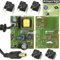
DESIGN ACCELERATOR KIT LP SWITCH
Manufacturer
Power Integrations
Series
LinkSwitch®-LPr
Specifications of DAK-85
Main Purpose
AC/DC, Primary Side
Outputs And Type
1, Isolated
Power - Output
2W
Voltage - Output
6V
Current - Output
330mA
Voltage - Input
90 ~ 265VAC
Regulator Topology
Flyback
Frequency - Switching
66kHz
Board Type
Bare (Unpopulated) and Fully Populated
Utilized Ic / Part
LNK562, LNK563, LNK564
Lead Free Status / RoHS Status
Lead free / RoHS Compliant
Other names
596-1104
Available stocks
Company
Part Number
Manufacturer
Quantity
Price
Company:

Part Number:
DAK-85
Manufacturer:
Power Integrations
Quantity:
135


NOTES:
A. In a scheme using a resistor divider network at the FB pin, where R
B. Total current consumption is the sum of I
C Since the output MOSFET is switching, it is diffi cult to isolate the switching current from the supply current at the
D. See Typical Performance Characteristics section Figure 16 for BYPASS pin startup charging waveform.
E. This current is only intended to supply an optional optocoupler connected between the BYPASS and FEEDBACK
F. This parameter is guaranteed by design.
G. This parameter is derived from characterization.
H. Breakdown voltage may be checked against minimum BV
Rev. H 11/08
FEEDBACK Pin
Auto-Restart
Threshold Voltage
Auto-Restart
ON-Time
Auto-Restart
Duty Cycle
10
OUTPUT (cont.)
bias voltage and R
by V
can be used:
To determine the contribution from I
Since I
switching) and the sum of I
DRAIN. An alternative is to measure the BYPASS pin current at 6 V.
pins and not any other external circuitry.
exceeding minimum BV
Parameter
FB
and I
FB
LNK562-564
and V
FB
variations. To determine the contribution from the V
FB
are independent parameters, the composite variation in percent would be
L
is the resistor from the FB pin to the SOURCE pin, the output voltage variation is infl uenced
Symbol
DSS
V
DC
FB(AR)
.
S2
AR
and I
x = 100 #
y = 100 #
DSS
SOURCE = 0 V; T
FB
when FEEDBACK pin is shorted to SOURCE (MOSFET switching).
variation in percent, the following equation can be used:
(Unless Otherwise Specifi ed)
S1
J
K
K
K K
L
J
K
K
K K
L
and I
V
V
V
V
FB(MAX)
FB(TYP)
FB(TYP)
FB(TYP)
Conditions
See Figure 8
V
T
T
DSS
FB
J
J
= 25 °C
= 25 °C
c
= V
c
c
c
when FEEDBACK pin voltage is ≥2 V (MOSFET not
R
R
R
R
J
U
U
U
U
FB(AR)
= -40 to 125 °C
R
R
+ R
R
R
+ R
+ R
+ R
L
L
L
L
DSS
L
L
L
L
m
m
m
by ramping the DRAIN pin voltage up to but not
m
+ I
+ I
+ I
+ I
FB
FB(MAX)
FB(TYP)
FB(TYP)
FB(TYP)
U
variation in percent, the following equation
is the resistor from the FB pin to the rectifi ed
R
R
R
R
U
U
U
U
- 1
- 1
Min
N
O
O
O O
P
N
O
O
O O
P
Typ
100
0.8
12
! x
Max
2
+ y
2
.
Units
ms
%
V
Related parts for DAK-85
Image
Part Number
Description
Manufacturer
Datasheet
Request
R

Part Number:
Description:
KIT DESIGN ACCELERATOR MODEM
Manufacturer:
Power Integrations
Datasheet:

Part Number:
Description:
KIT DESIGN ACCELERATOR SET TOP
Manufacturer:
Power Integrations
Datasheet:

Part Number:
Description:
KIT REF DES DPA 6.6W DC-DC CONV
Manufacturer:
Power Integrations
Datasheet:

Part Number:
Description:
KIT DESIGN ACCELERATOR POE CONV
Manufacturer:
Power Integrations
Datasheet:

Part Number:
Description:
DESIGN ACCELERATOR KIT XT SWITCH
Manufacturer:
Power Integrations
Datasheet:

Part Number:
Description:
KIT DESIGN ACC PEAKSWITCH FAMILY
Manufacturer:
Power Integrations
Datasheet:

Part Number:
Description:
KIT DESIGN ACCELERATOR ADAPTER
Manufacturer:
Power Integrations
Datasheet:

Part Number:
Description:
KIT DESIGN ACCELERATOR ADAPTER
Manufacturer:
Power Integrations
Datasheet:

Part Number:
Description:
KIT DESIGN ACCELERATOR DC-DC
Manufacturer:
Power Integrations
Datasheet:

Part Number:
Description:
KIT DESIGN ACCELERATOR DPA SW
Manufacturer:
Power Integrations
Datasheet: