MCP1630DM-DDBS2 Microchip Technology, MCP1630DM-DDBS2 Datasheet - Page 8
MCP1630DM-DDBS2
Manufacturer Part Number
MCP1630DM-DDBS2
Description
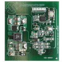
BOARD DEMO BOOST COUPLED INDUCTR
Manufacturer
Microchip Technology
Type
DC/DC Switching Converters, Regulators & Controllersr
Specifications of MCP1630DM-DDBS2
Main Purpose
DC/DC, Step Up
Outputs And Type
1, Non-Isolated
Voltage - Output
15 ~ 40V
Current - Output
30mA
Voltage - Input
3 ~ 5.5V
Regulator Topology
Boost
Frequency - Switching
100kHz
Board Type
Fully Populated
Utilized Ic / Part
MCP1630
Output Voltage
15 V to 40 V
Product
Power Management Modules
For Use With/related Products
MCP1630, PIC12F683
Lead Free Status / RoHS Status
Not applicable / Not applicable
Power - Output
-
Lead Free Status / Rohs Status
Lead free / RoHS Compliant


MCP1630/MCP1630V
2.0
Note: Unless otherwise noted, V
values = 5.0V, T
FIGURE 2-1:
Input Voltage.
FIGURE 2-2:
Input Voltage.
FIGURE 2-3:
Response.
DS21896B-page 8
Note:
-10
-12
-14
3.5
2.5
1.5
0.5
4.5
3.5
2.5
1.5
0.5
1000000
-2
-4
-6
-8
2
0
3
2
1
0
4
3
2
1
0
1M
TYPICAL PERFORMANCE CURVES
F
F
The graphs and tables provided following this note are a statistical summary based on a limited number of
samples and are provided for informational purposes only. The performance characteristics listed herein
are not tested or guaranteed. In some graphs or tables, the data presented may be outside the specified
operating range (e.g., outside specified power supply range) and therefore outside the warranted range.
OSC IN
OSC IN
V
R
C
REF
LOAD
LOAD
= DC
A
= 1 MHz
= 2V
= 4.7 k
= 67 pF
= -40°C to +125°C.
Phase
T
Gain
A
Frequency (Hz)
= - 40°C
T
A
Input Quiescent Current vs.
Input Quiescent Current vs.
Error Amplifier Frequency
= - 40°C
Input Voltage (V)
Input Voltage (V)
T
A
T
= + 125°C
A
T
= + 125°C
A
5M
= + 25°C
T
IN
A
= + 25°C
= 3.0V to 5.5V, F
10000000
10M
250
200
150
100
50
0
OSC
= 1 MHz with 10% Duty Cycle, C
FIGURE 2-4:
Current vs. Input Voltage.
FIGURE 2-5:
vs. Input Voltage.
FIGURE 2-6:
Current vs. Input Voltage.
18
16
14
12
10
8
6
4
2
0
-100
-10
-12
-14
700
600
500
400
300
200
100
-2
-4
-6
-8
0
0
V
CM
= V
IN
Error Amplifier Input Bias
Error Amplifier Sink Current
Error Amplifier Source
Input Voltage (V)
© 2005 Microchip Technology Inc.
Input Voltage (V)
Input Voltage (V)
T
T
T
A
A
A
T
= - 40°C
= + 25°C
= + 125°C
T
IN
A
A
= - 40°C
= + 125°C
= 0.1 µF, V
T
T
T
A
A
A
= + 125°C
= + 25°C
= - 40°C
T
A
= + 85°C
T
IN
A
= + 25°C
for typical
Related parts for MCP1630DM-DDBS2
Image
Part Number
Description
Manufacturer
Datasheet
Request
R

Part Number:
Description:
BOARD DEMO BOOST AUTO INPUT
Manufacturer:
Microchip Technology
Datasheet:

Part Number:
Description:
BOARD CONV DEMO MCP1630 TRPL-OUT
Manufacturer:
Microchip Technology
Datasheet:

Part Number:
Description:
BOARD DEMO FOR MCP1630
Manufacturer:
Microchip Technology
Datasheet:

Part Number:
Description:
BOARD DEMO MCP1630 BIAS SUPPLY
Manufacturer:
Microchip Technology
Datasheet:

Part Number:
Description:
BOARD DEM MCP1630 BOOST MODE LED
Manufacturer:
Microchip Technology
Datasheet:

Part Number:
Description:
Manufacturer:
Microchip Technology Inc.
Datasheet:
Part Number:
Description:
Manufacturer:
Microchip Technology Inc.
Datasheet:
Part Number:
Description:
Manufacturer:
Microchip Technology Inc.
Datasheet:
Part Number:
Description:
Manufacturer:
Microchip Technology Inc.
Datasheet:
Part Number:
Description:
Manufacturer:
Microchip Technology Inc.
Datasheet:
Part Number:
Description:
Manufacturer:
Microchip Technology Inc.
Datasheet: