CRD35L01 Cirrus Logic Inc, CRD35L01 Datasheet
CRD35L01
Specifications of CRD35L01


Related parts for CRD35L01


CRD35L01 Summary of contents
Page 1
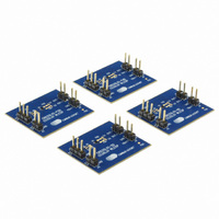
... Input (J1) Shutdown Control (J2) http://www.cirrus.com Description The CRD35L01 demonstrates the CS35L01 high-effi- ciency Hybrid Class-D audio amplifier. This reference design implements a single-channel amplifier that deliv- ers 1.7 W per full-bridge channel into 8- loads using a single +5-V supply. Differential audio inputs can easily be connected through the J1 header ...
Page 2
... Figure 19.CRD35L01-HD Bottom Side Component Placement ................................................................ 12 Figure 20.CRD35L01-HD Layer 1 Copper ................................................................................................ 12 Figure 21.CRD35L01-HD Layer 2 Copper ................................................................................................ 12 Figure 22.CRD35L01-HD Layer 3 Copper ................................................................................................ 12 Figure 23.CRD35L01-HD Layer 4 Copper ................................................................................................ 12 Figure 24.CRD35L01-FHD Top Side Component Placement ................................................................... 13 Figure 25.CRD35L01-FHD Bottom Side Component Placement ............................................................. 13 Figure 26.CRD35L01-FHD Layer 1 Copper .............................................................................................. 13 Figure 27.CRD35L01-FHD Layer 2 Copper .............................................................................................. 13 Figure 28.CRD35L01-FHD Layer 3 Copper .............................................................................................. 13 Figure 29 ...
Page 3
... LIST OF TABLES Table 1. System Input and Output Connections ......................................................................................... 7 Table 2. J2 Shutdown Control Settings ....................................................................................................... 7 Table 3. Bill of Materials Listing .................................................................................................................. 9 DS914RD2 CRD35L01 3 ...
Page 4
... Power Supply A single +2.5 to +5.5 VDC power supply is required to power the CRD35L01. The supply must be capable of delivering sufficient current for the intended power output. The supply provides power to the CS35L01. The power supply connection to the board is provided by the header J4. The positive terminal is labeled VBATT ...
Page 5
... The location of these required cuts are shown in Cut the bypass traces before insert- ing the optional input gain adjust- ment resistors Figure 1. Optional Bypass Trace Cut Locations DS914RD2 CRD35L01 Figure 1. After the trace between the Figure 3 on Figure 1. Cut the bypass traces before insert- ...
Page 6
... The CS35L01 requires careful attention to power supply and grounding arrangements to optimize performance and minimize radiated emissions. The decoupling capacitors should be located as close to the CS35L01 as possible. This can be optimized by using both top and bottom side component population as demonstrated by the CRD35L01 boards. 2.1 Power Supply Decoupling Proper power supply decoupling is one key to maximizing the performance of a Class-D amplifier ...
Page 7
... Analog output (-) from CS35L01. Input Positive connection from power supply, +2.5 to +5.5 VDC. Input GND connection from power supply. Table 1. System Input and Output Connections Low = CS35L01 shutdown enabled High = CS35L01 shutdown disabled Table 2. J2 Shutdown Control Settings CRD35L01 Connector Function Function Selected 7 ...
Page 8
... CRD SCHEMATIC 8 CRD35L01 DS914RD2 ...
Page 9
... Bill of Materials The component listing below is shown for the four CRD35L01 board variations (-SD, -FSD, -HD, and -FHD). Unpopulated (DNP) components are listed with recommended components for reference purposes. Reference Qty Designator(s) CRD35L01 Boards 2 C1, C2 -SD, -FSD, -HD, -FHD 1 C3 -SD, -FSD, -HD, -FHD 1 C6 ...
Page 10
... CRD LAYOUT Figure 6. CRD35L01-SD Top Side Component Placement Figure 8. CRD35L01-SD Layer 1 Copper Figure 10. CRD35L01-SD Layer 3 Copper 10 Figure 7. CRD35L01-SD Bottom Side Component Placement Figure 9. CRD35L01-SD Layer 2 Copper Figure 11. CRD35L01-SD Layer 4 Copper CRD35L01 DS914RD2 ...
Page 11
... Figure 12. CRD35L01-FSD Top Side Component Placement Figure 14. CRD35L01-FSD Layer 1 Copper Figure 16. CRD35L01-FSD Layer 3 Copper DS914RD2 Figure 13. CRD35L01-FSD Bottom Side Component Placement Figure 15. CRD35L01-FSD Layer 2 Copper Figure 17. CRD35L01-FSD Layer 4 Copper CRD35L01 11 ...
Page 12
... Figure 18. CRD35L01-HD Top Side Component Placement Figure 20. CRD35L01-HD Layer 1 Copper Figure 22. CRD35L01-HD Layer 3 Copper 12 Figure 19. CRD35L01-HD Bottom Side Component Placement Figure 21. CRD35L01-HD Layer 2 Copper Figure 23. CRD35L01-HD Layer 4 Copper CRD35L01 DS914RD2 ...
Page 13
... Figure 24. CRD35L01-FHD Top Side Component Placement Figure 26. CRD35L01-FHD Layer 1 Copper Figure 28. CRD35L01-FHD Layer 3 Copper DS914RD2 Figure 25. CRD35L01-FHD Bottom Side Compo- nent Placement Figure 27. CRD35L01-FHD Layer 2 Copper Figure 29. CRD35L01-FHD Layer 4 Copper CRD35L01 13 ...
Page 14
... Updated Figure 5 on page 8 – Updated BOM values for C6 & the typical connection diagram in the DS909A2 datasheet. All CRD35L01-SD, -FSD, -HD, and -FHD boards with an assembly date of 02/15/10 or earlier contain components from the Rev A0 BOM. Contacting Cirrus Logic Support For all product questions and inquiries, contact a Cirrus Logic Sales Representative. ...