CDB5361 Cirrus Logic Inc, CDB5361 Datasheet - Page 19
CDB5361
Manufacturer Part Number
CDB5361
Description
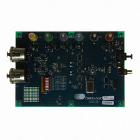
BOARD EVAL FOR CS5361 STEREO ADC
Manufacturer
Cirrus Logic Inc
Specifications of CDB5361
Number Of Adc's
2
Number Of Bits
24
Sampling Rate (per Second)
192k
Data Interface
Serial
Inputs Per Adc
1 Differential
Power (typ) @ Conditions
198mW @ 5 V
Voltage Supply Source
Analog and Digital
Operating Temperature
-10°C ~ 70°C
Utilized Ic / Part
CS5361
Product
Audio Modules
Lead Free Status / RoHS Status
Contains lead / RoHS non-compliant
Lead Free Status / RoHS Status
Lead free / RoHS Compliant, Contains lead / RoHS non-compliant
Other names
598-1547


4.5
The operational amplifiers in the input circuitry driving the CS5361 may generate a small DC offset into the A/D con-
verter. The CS5361 includes a high-pass filter after the decimator to remove any DC offset which could result in re-
cording a DC level, possibly yielding “clicks” when switching between devices in a multichannel system.
The high-pass filter continuously subtracts a measure of the DC offset from the output of the decimation filter. If the
HPF pin is taken high during normal operation, the current value of the DC offset register is frozen and this DC offset
will continue to be subtracted from the conversion result. This feature makes it possible to perform a system DC
offset calibration by:
A system calibration performed in this way will eliminate offsets anywhere in the signal path between the calibration
point and the CS5361.
4.6
The CS5361 includes overflow detection on both the left and right channels. This time multiplexed information is
presented as open drain, active low on pin 15, OVFL. The OVFL_L and OVFL_R data will go to a logical low as soon
as an overrange condition in either channel is detected. The data will remain low as specified in the Switching Char-
acteristics - Serial Audio Port section. This ensures sufficient time to detect an overrange condition regardless of the
speed mode. After the timeout, the OVFL_L and OVFL_R data will return to a logical high if there has not been any
other overrange condition detected. Please note that an overrange condition on either channel will restart the time-
out period for both channels.
4.6.1
In left-justified format, the OVFL pin is updated one SCLK period after an LRCK transition. In I
pin is updated two SCLK periods after an LRCK transition. Refer to Figures 23 and 24. In both cases the OVFL data
can be easily demultiplexed by using the LRCK to latch the data. In left-justified format, the rising edge of LRCK
would latch the right channel overflow status, and the falling edge of LRCK would latch the left channel overflow
status. In I
LRCK would latch the left channel overflow status.
4.7
As with any high resolution converter, the CS5361 requires careful attention to power supply and grounding arrange-
ments if its potential performance is to be realized. Figure 22 shows the recommended power arrangements, with
VA and VL connected to clean supplies. VD, which powers the digital filter, may be run from the system logic supply
or may be powered from the analog supply via a resistor. In this case, no additional devices should be powered from
VD. Decoupling capacitors should be as near to the ADC as possible, with the low value ceramic capacitor being
the nearest. All signals, especially clocks, should be kept away from the FILT+ and VQ pins in order to avoid un-
wanted coupling into the modulators. The FILT+ and VQ decoupling capacitors, particularly the 0.01 µF, must be
positioned to minimize the electrical path from FILT+ and REFGND. The CDB5361 evaluation board demonstrates
the optimum layout and power supply arrangements. To minimize digital noise, connect the ADC digital outputs only
to CMOS inputs.
4.8
In systems where multiple ADCs are required, care must be taken to achieve simultaneous sampling. To ensure
synchronous sampling, the MCLK and LRCK must be the same for all of the CS5361’s in the system. If only one
master clock source is needed, one solution is to place one CS5361 in Master mode, and slave all of the other
CS5361’s to the one master. If multiple master clock sources are needed, a possible solution would be to supply all
clocks from the same external source and time the CS5361 reset with the inactive edge of MCLK. This will ensure
that all converters begin sampling on the same clock edge.
DS467F2
1) Running the CS5361 with the high-pass filter enabled until the filter settles. See the Digital Filter Character-
2) Disabling the high-pass filter and freezing the stored DC offset.
istics for filter settling time.
Overflow Detection
Grounding and Power Supply Decoupling
Synchronization of Multiple Devices
High-pass Filter and DC Offset Calibration
OVFL Output Timing
2
S format, the falling edge of LRCK would latch the right channel overflow status and the rising edge of
2
S format, the OVFL
CS5361
19
Related parts for CDB5361
Image
Part Number
Description
Manufacturer
Datasheet
Request
R

Part Number:
Description:
Development Kit
Manufacturer:
Cirrus Logic Inc
Datasheet:
Part Number:
Description:
Development Kit
Manufacturer:
Cirrus Logic Inc
Datasheet:


Part Number:
Description:
High-efficiency PFC + Fluorescent Lamp Driver Reference Design
Manufacturer:
Cirrus Logic Inc
Datasheet:
Part Number:
Description:
Development Kit
Manufacturer:
Cirrus Logic Inc
Datasheet:
Part Number:
Description:
Development Kit
Manufacturer:
Cirrus Logic Inc
Datasheet:

Part Number:
Description:
Development Kit
Manufacturer:
Cirrus Logic Inc
Datasheet:
Part Number:
Description:
Development Kit
Manufacturer:
Cirrus Logic Inc
Datasheet:
Part Number:
Description:
Development Kit
Manufacturer:
Cirrus Logic Inc
Datasheet:
Part Number:
Description:
Development Kit
Manufacturer:
Cirrus Logic Inc
Datasheet:

Part Number:
Description:
EVALUATION BOARD FOR CS8427
Manufacturer:
Cirrus Logic Inc
Datasheet:

Part Number:
Description:
BOARD EVAL FOR CS8416 RCVR
Manufacturer:
Cirrus Logic Inc
Datasheet:

Part Number:
Description:
EVALUATION BOARD FOR CS8420
Manufacturer:
Cirrus Logic Inc
Datasheet:

Part Number:
Description:
KIT DEVELOPMENT EP9315 ARM9
Manufacturer:
Cirrus Logic Inc
Datasheet:

Part Number:
Description:
KIT DEVELOPMENT EP9302 ARM9
Manufacturer:
Cirrus Logic Inc
Datasheet: