CDB5381 Cirrus Logic Inc, CDB5381 Datasheet - Page 18
CDB5381
Manufacturer Part Number
CDB5381
Description
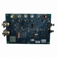
BOARD EVAL FOR CS5381 192KHZ ADC
Manufacturer
Cirrus Logic Inc
Specifications of CDB5381
Number Of Adc's
2
Number Of Bits
24
Sampling Rate (per Second)
192k
Data Interface
Serial
Inputs Per Adc
1 Differential
Input Range
6.1 Vpp
Power (typ) @ Conditions
360mW @ 5 V
Voltage Supply Source
Analog and Digital
Operating Temperature
-10°C ~ 70°C
Utilized Ic / Part
CS5381
Product
Audio Modules
Lead Free Status / RoHS Status
Contains lead / RoHS non-compliant
Lead Free Status / RoHS Status
Lead free / RoHS Compliant, Contains lead / RoHS non-compliant
Other names
598-1008


18
3.6
3.6.1
3.6.2
3.7
3.8
Overflow Detection
The CS5381 includes overflow detection on both the left and right channels. This time multiplexed informa-
tion is presented as open drain, active low on pin 15, OVFL. The OVFL_L and OVFL_R data will go to a
logical low as soon as an overrange condition in the opposite channel is detected. The data will remain low
as specified in the
time to detect an overrange condition regardless of the speed mode. After the timeout, the OVFL_L and
OVFL_R data will return to a logical high if there has not been any other overrange condition detected.
Please note that an overrange condition on either channel will restart the timeout period for both channels.
Grounding and Power Supply Decoupling
As with any high resolution converter, the CS5381 requires careful attention to power supply and grounding
arrangements if its potential performance is to be realized.
rangements, with VA and VL connected to clean supplies. VD, which powers the digital filter, may be run
from the system logic supply or may be powered from the analog supply via a resistor. In this case, no ad-
ditional devices should be powered from VD. Decoupling capacitors should be as near to the ADC as pos-
sible, with the low value ceramic capacitor being the nearest. All signals, especially clocks, should be kept
away from the FILT+ and VQ pins in order to avoid unwanted coupling into the modulators. The FILT+ and
VQ decoupling capacitors, particularly the 0.01 µF, must be positioned to minimize the electrical path from
FILT+ and REFGND. The CDB5381 evaluation board demonstrates the optimum layout and power supply
arrangements. To minimize digital noise, connect the ADC digital outputs only to CMOS inputs.
Synchronization of Multiple Devices
In systems where multiple ADCs are required, care must be taken to achieve simultaneous sampling. To
ensure synchronous sampling, the MCLK and LRCK must be the same for all of the CS5381’s in the system.
If only one master clock source is needed, one solution is to place one CS5381 in Master mode, and slave
all of the other CS5381’s to the one master. If multiple master clock sources are needed, a possible solution
would be to supply all clocks from the same external source and time the CS5381 reset with the falling edge
of MCLK. This will ensure that all converters begin sampling on the same clock edge.
OVFL Configuration
If the system does not require overflow detection, the user may leave the OVFL pin disconnected. When
using the overflow detection capability of the CS5381, a 10 kΩ pull-up resistor must be inserted between
the OVFL pin and VL because the OVFL output is open drain, active low. This means that the OVFL pin
is high impedance for the case of no overflow condition, but the pull-up resistor will pull the node to VL.
When an overflow condition occurs, the OVFL pin can drive the node to GND thus indicating the presence
of the overflow condition. In effect, the user can use the OVFL pin to illuminate an LED, or mute the chan-
nel with an external circuit or a DSP. Furthermore, because the OVFL output is open-drain, the OVFL pins
of multiple CS5381 devices can be tied together such that an overflow condition on a single device will
drive the line low. When connecting OVFL pins of multiple devices, only a single 10kΩ pull-up resistor is
necessary.
OVFL Output Timing
In left-justified format, the OVFL pin is updated one SCLK period after an LRCK transition. In I²S format,
the OVFL pin is updated two SCLK periods after an LRCK transition. Refer to
cases, the OVFL data can be easily demultiplexed by using the LRCK to latch the data. In left-justified
format, the rising edge of LRCK would latch the right channel overflow status, and the falling edge of
LRCK would latch the left channel overflow status. In I²S format, the falling edge of LRCK would latch the
right channel overflow status and the rising edge of LRCK would latch the left channel overflow status.
“Switching Characteristics - Serial Audio Port” section on page
Figure 22
shows the recommended power ar-
Figures 20
10. This ensures sufficient
and 21. In both
CS5381
DS563F2
Related parts for CDB5381
Image
Part Number
Description
Manufacturer
Datasheet
Request
R

Part Number:
Description:
Development Kit
Manufacturer:
Cirrus Logic Inc
Datasheet:
Part Number:
Description:
Development Kit
Manufacturer:
Cirrus Logic Inc
Datasheet:


Part Number:
Description:
High-efficiency PFC + Fluorescent Lamp Driver Reference Design
Manufacturer:
Cirrus Logic Inc
Datasheet:
Part Number:
Description:
Development Kit
Manufacturer:
Cirrus Logic Inc
Datasheet:
Part Number:
Description:
Development Kit
Manufacturer:
Cirrus Logic Inc
Datasheet:

Part Number:
Description:
Development Kit
Manufacturer:
Cirrus Logic Inc
Datasheet:
Part Number:
Description:
Development Kit
Manufacturer:
Cirrus Logic Inc
Datasheet:
Part Number:
Description:
Development Kit
Manufacturer:
Cirrus Logic Inc
Datasheet:
Part Number:
Description:
Development Kit
Manufacturer:
Cirrus Logic Inc
Datasheet:

Part Number:
Description:
EVALUATION BOARD FOR CS8427
Manufacturer:
Cirrus Logic Inc
Datasheet:

Part Number:
Description:
BOARD EVAL FOR CS8416 RCVR
Manufacturer:
Cirrus Logic Inc
Datasheet:

Part Number:
Description:
EVALUATION BOARD FOR CS8420
Manufacturer:
Cirrus Logic Inc
Datasheet:

Part Number:
Description:
KIT DEVELOPMENT EP9315 ARM9
Manufacturer:
Cirrus Logic Inc
Datasheet:

Part Number:
Description:
KIT DEVELOPMENT EP9302 ARM9
Manufacturer:
Cirrus Logic Inc
Datasheet: